Because of the Thanksgiving holiday in the U.S., TI E2E™ design support forum responses may be delayed from November 25 through December 2. Thank you for your patience.

This thread has been locked.

If you have a related question, please click the "Ask a related question" button in the top right corner. The newly created question will be automatically linked to this question.

SN65HVD1176: Part is Destroyed when Switching from 0V to -7V on Terminal A

Part Number: SN65HVD1176

Hello,

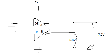
I'm trying to do the "Input voltage ranges" test specified in TIA-485-A. Therefore, I have to apply -7V to terminal A and -6.8V to terminal B of the transceiver (see Table 1 in section 4.3.2 of the standard). During the test the transceiver is on but the driver is disabled.

When I switch the power supplies on they ramp with approx. 70mV/us to the specified values, the transceiver is destroyed and I have a short circuit between Terminal A and GND. I get the same result when the transceiver is completely off. By now I destroyed multiple transceivers with this setup.

If I ramp up with less than 1V/s the transceiver is not harmed. But this doens't seem to be the idea of the test nor the "Recommended Operation Conditions" given in the data sheet.

Can somebody tell me what I'm doing wrong or where it's specified that it's not possible to switch "fast" from 0V to -7V in the data sheet?

In case it's not possible, how can this transceiver comply with TIA-485-A?

Regards,

Raphael

  • Raphael,

    The input voltage ranges of RS-485 transceivers show that the communication works with a wide common mode range. For example, if the voltage on A and B toggles between -6.8V to -7.0V (-6.9V common mode voltage), you expect the transceivers generate correct data. I'm not sure why you ramp up the supply after the voltage is applied to the wire. In some applications, an extra node is added to an existing bus. However usually the node supply is ready before the module connects to the main bus (hot plug-in). Please let me know if you have more questions about the spec or application. 

    Regards,

    Hao

  • Hi Hao,

    It doesn't matter if I ramp up and the wire is already plugged in or if I start the supplies and plug in the wire. In both setup the transceiver is destroyed. Since our product (with your transceiver) has to be compliant with TIA-RS485 it doesn't matter for us if it is not a normal usecase as long as it is specified in the standard.

    To clarify my setup, here a sketch:

    In further tests I found out that it happens even more often when I apply first Va=12V, Vb=11.8V, then switch off the supplies and then apply Va=-7V and Vb =-6.8V.

    Regards,

    Raphael

  • Raphael,

    The sketch helps. Is it possible for you to monitor the bus voltage in the tests? I suspect that somehow the voltage doesn't settle down as quickly as you expected. If overshoot or undershoot happened and the pin voltage went beyond the specified abs max, the device could be damaged.

    In application, this is how the input range is tested. You start with the normal operation (for example: 5V supply, 100kbps PRBS data), then change the common mode of the bus to -7V or 12V to see if the communication is still successful.  

    You can refer to figure 10 on page 11 of this datasheet for the common mode voltage check for the driver. I hope it be helpful.

    www.ti.com/.../sllse11h.pdf

    Please let me know if you have further questions.

    Regards,

    Hao

  • Hi Hao

    Here the monitored voltages during the test:

    I applied first 12V / 11.8V, then shut the supplies down and applied -7V / -6.8V and the -7V supply triggers the current limiter since I have a short between terminal A and GND. Vb goes up approx. 1s after Va, since the power supply reacts slower. Nevertheless, I'm always within +-12V Vdiff (Va - Vb) and this should not harm the transceiver.

    Compared to Figure 10 of the data sheet I don't have the 375Ohm series resistors, but those are not specified in TIA-485-A either. What  voltage steps are applied to the transceiver in Figure 10? Since it is only written -7V < V(test) < 12V.

    Thanks for your help

    Regards,

    Raphael

  • Raphael,

    Thanks for your information. I was asking if you saved the waveforms in the tests that destroyed the parts. For example, apply -7V to terminal A and -6.8V to terminal B, then ramp up Vcc with 70mV/us rate to 5V. Can you also confirm the state of logic pins, like D=0V, DE=0V, etc? If you want, we can discuss the issue directly with the help of TI field application engineer.

    Regards,

    Hao

  • Raphael,

    I'm closing this ticket per out offline discussion. Please let me know if you have more questions.

    Regards,

    Hao