Hello,
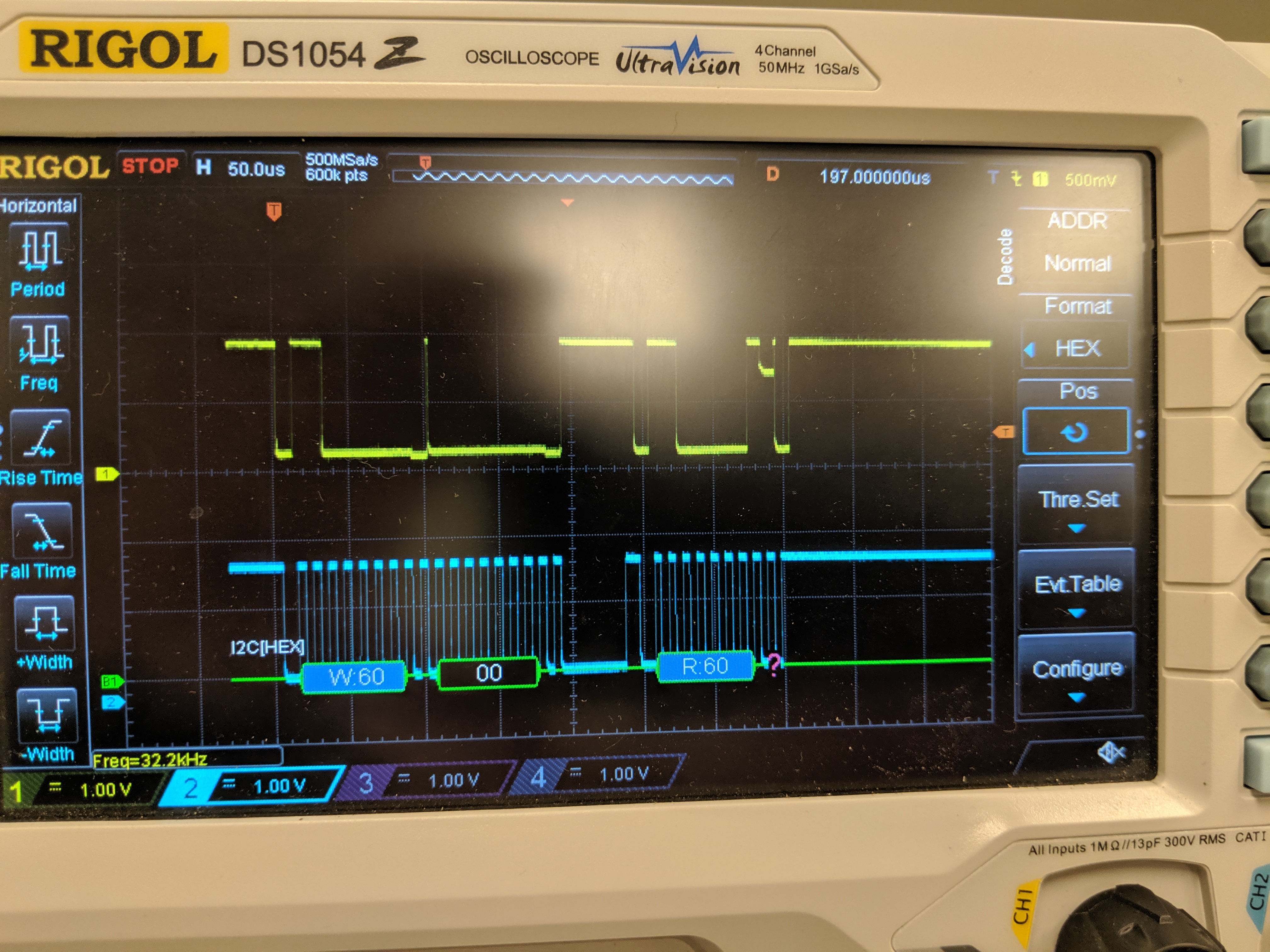
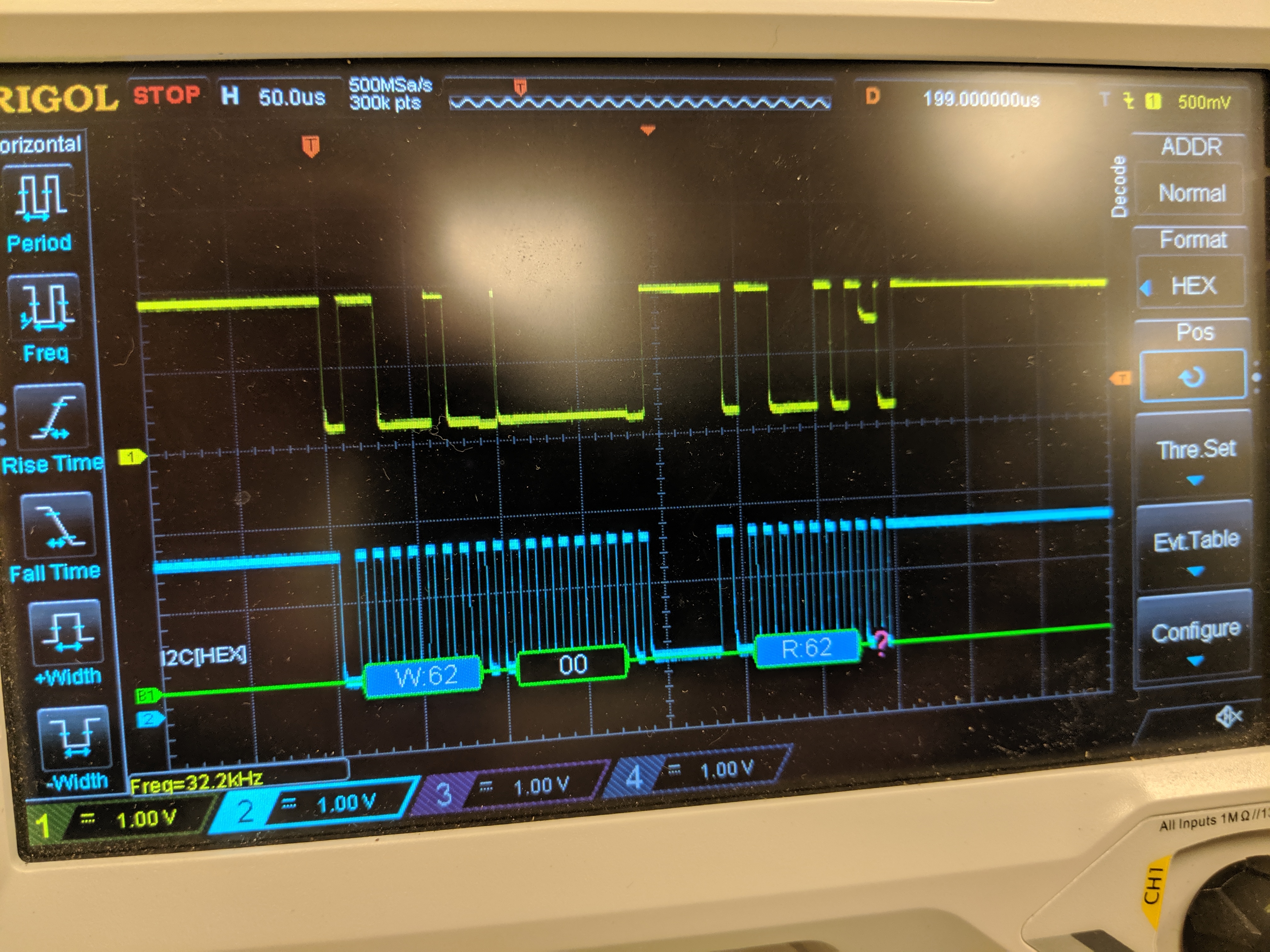
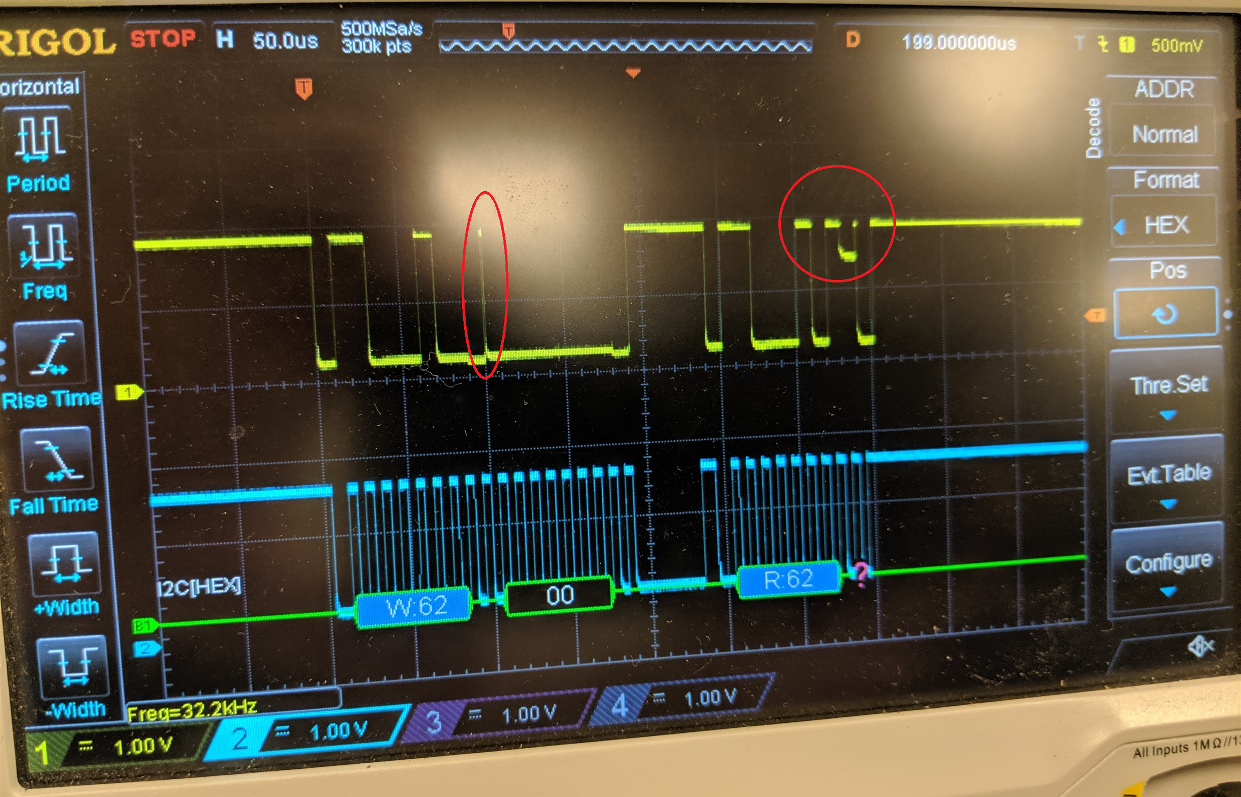
We have (16) DS90UB914ATRHS-Q1 on the same i2c bus. We can see that valid, clean i2c traffic is arriving at the sda and scl pins of each of the devices on the board. The bus is running at 100khz. Upon doing an i2cdetect -y -a -r in Linux, we are only seeing a sub-set of the de-serializers. Below is the output. We would expect there to be a deserializer at 0x60 - 0x6F per table 6 of the datasheet ( http://www.ti.com/lit/ds/symlink/ds90ub914a-q1.pdf ).
# i2cdetect -y -a -r 0
0 1 2 3 4 5 6 7 8 9 a b c d e f
00: -- -- -- -- -- -- -- -- -- -- -- -- 0c -- -- --
10: -- -- -- -- -- -- -- -- 18 19 -- -- -- -- -- --
20: -- -- -- -- -- -- -- -- -- -- -- -- -- -- -- 2f
30: -- -- -- -- -- -- -- -- -- -- -- -- -- -- -- --
40: -- -- -- -- -- -- -- -- -- -- -- -- -- -- -- --
50: -- -- -- -- -- -- -- -- -- -- -- -- -- -- -- --
60: -- -- -- 63 -- -- -- 67 -- -- -- -- 6c 6d -- 6f
70: -- -- -- -- -- -- -- -- -- -- -- -- -- -- -- --
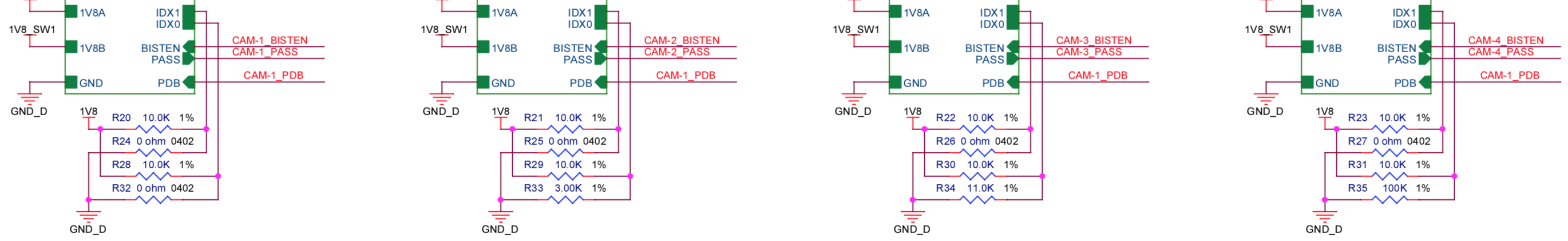
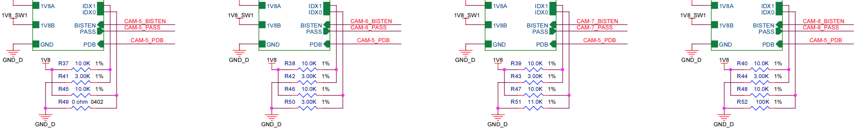
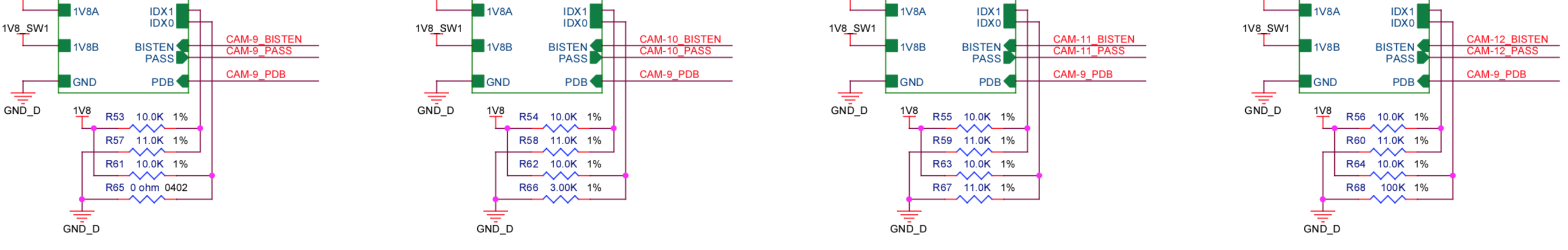
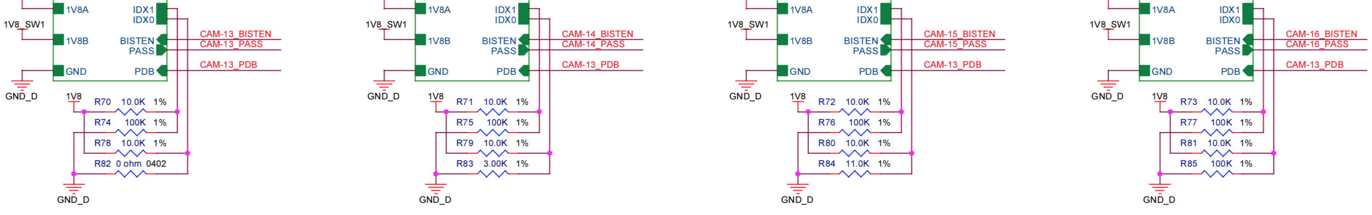
When reading register 0x00 from 0x63, 0x67, 0x6c, 0x6d, and 0x6f, they all return 0xC0 ( inferring they all believe that their ID is set from the IDx[0]and IDx[1] pins, but have an address of 0x60.
Additionally, with no serializer attached and bisten de-asserted, some of the devices have one or both of LOCK and PASS asserted high. On reboot, the same devices have the same level for LOCK and PASS. Viewing on the scope shows these pins are not toggling, and steady state.
We are using the RIN0 pair, with the RIN1 floating to test points.
GPIO0 - GPIO3 are pulled to GND via a 100k resistors.
SDA and SCL are driven from a TCA9803DGKR with no pull-ups on the "B side" of the buss. The "A side" has 2k pull ups.
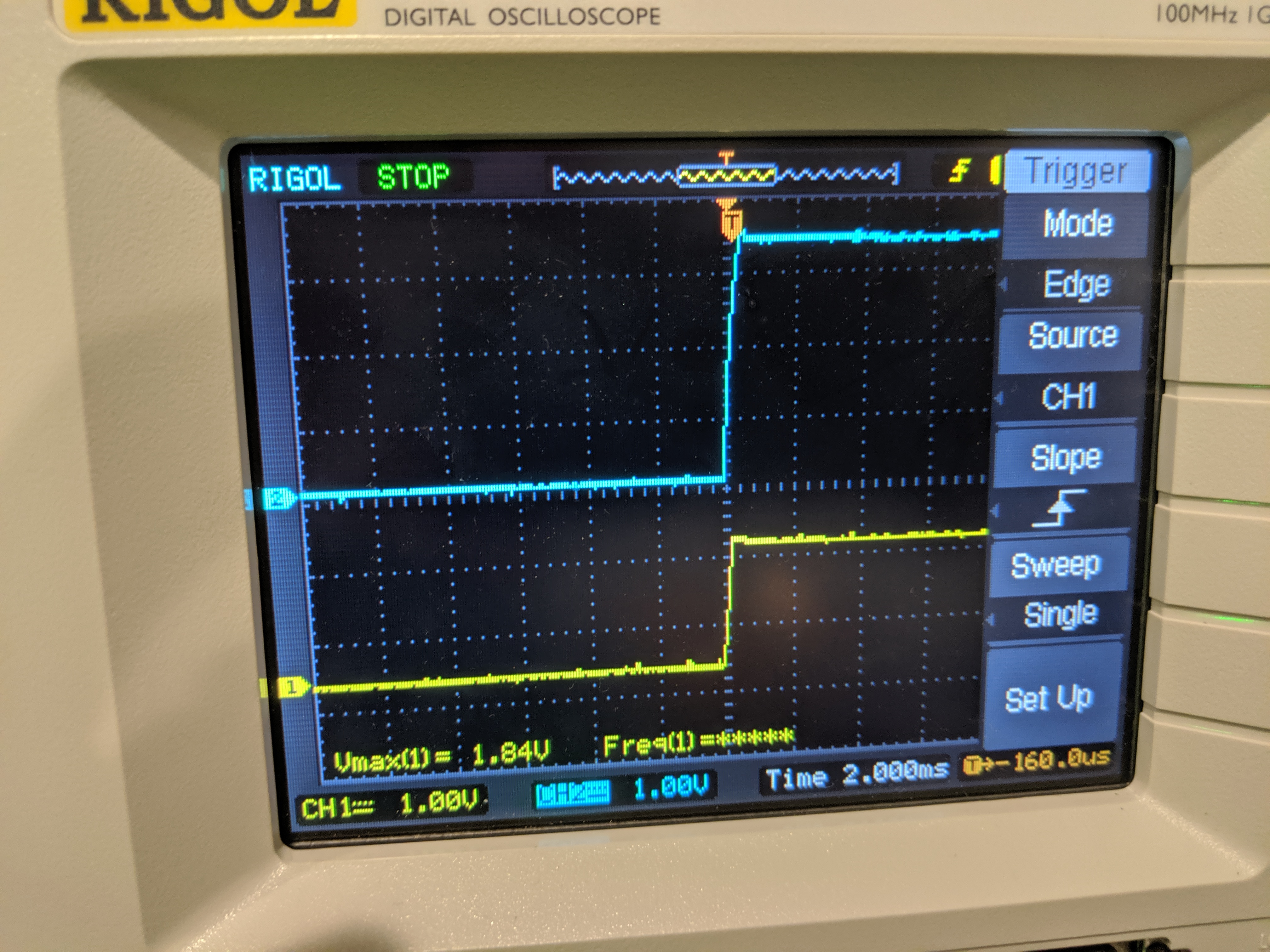
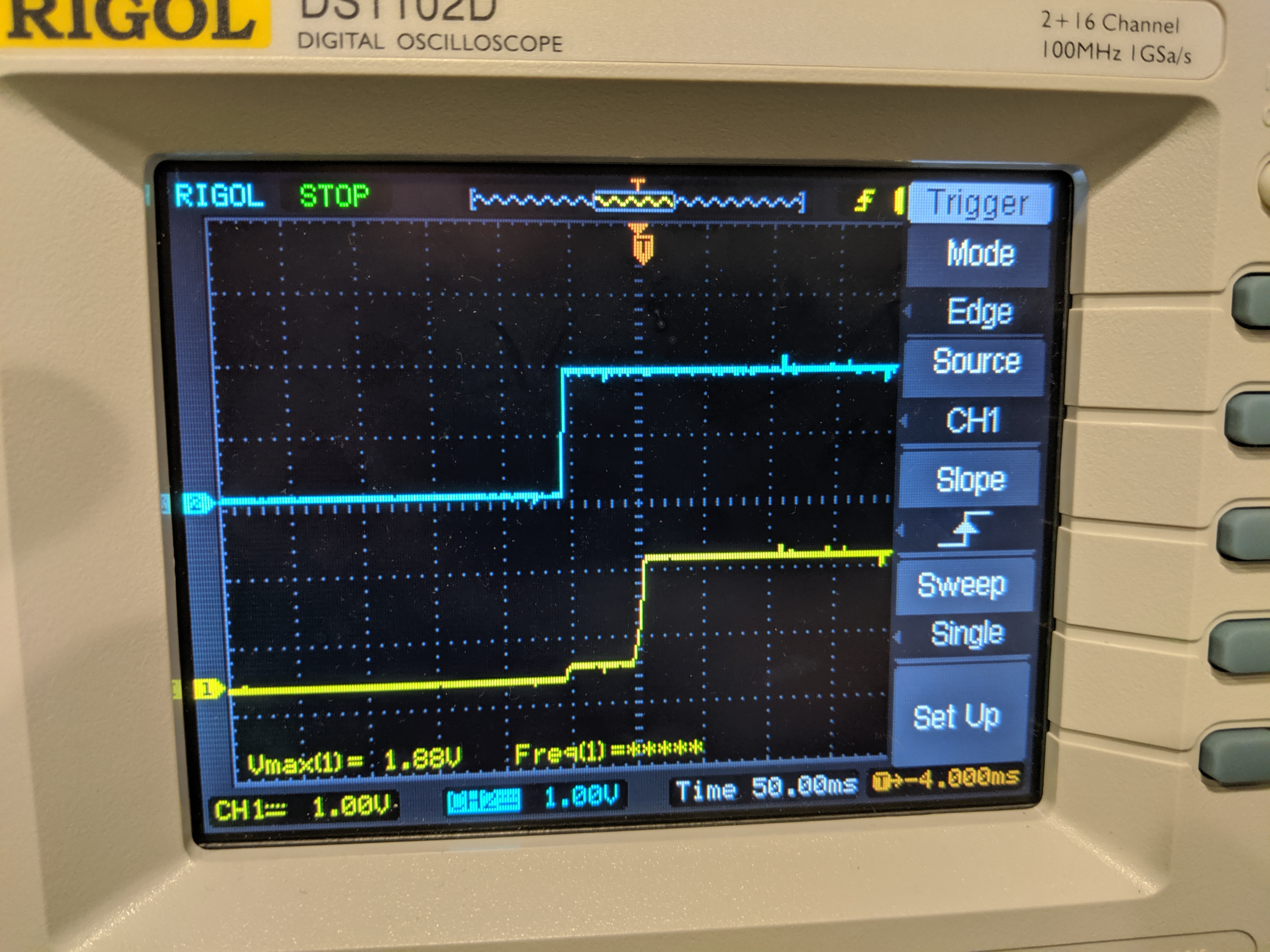
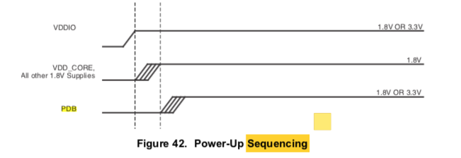
VDDIO1, VDDIO2, VDDIO3 are pulled to a 1.8v rail ( 1V8A ), and VDDD, VDDSSCG, VDDR, VDDCML0, VDDCML1, and VDDPLL are pulled to a different 1.8v rail (1V8B ). VSS is pulled to a shared ground. The timing of the two 1.8v rails is 1V8A comes up first, then 1V8B after. The time between the two is hundreds of microseconds.
PDB is, for ~100ms floating before being driven high ( this is due to the configuration time of an FPGA, and the net does not have a pull down on it ).
MODE is set with a resistor divider of RMODE is set to 11k per table for 10 bit mode ( note: it has been identified this needs to be 0 ohms to work with our serializer and clock, however I would not expect that to impact the i2c traffic functionality in this manor )
BISTEN is, for ~100ms floating before being driven low ( this is due to the configuration time of the FPGA, and the net does not have a pull down on it ).
SEL is pulled low.
OSS_SEL and OEN is pulled high to 1V8A.
Is there something that sticks out as being very wrong? This design was validated on the EVM for the deserialize with just one device on the bus, and everything worked as expected.
Thank you,
-TD