This thread has been locked.

If you have a related question, please click the "Ask a related question" button in the top right corner. The newly created question will be automatically linked to this question.

DS90CR288A: CMOS/TTL output setup hold time

Part Number: DS90CR288A

Hi Team,

I have a confirmation with DS90CR288A.

Customers are evaluating DS90CR288A.
I think that the setup hold time is not kept in the output waveform of CMOS / TTL.
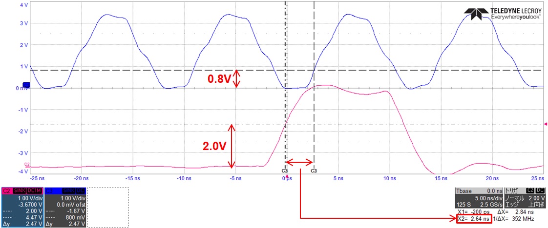
Below is the waveform measured by the customer.

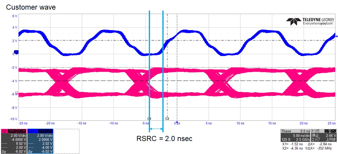
The data sheet spec says 3.5nsec, but it is output below the spec.
Is this spec correct?


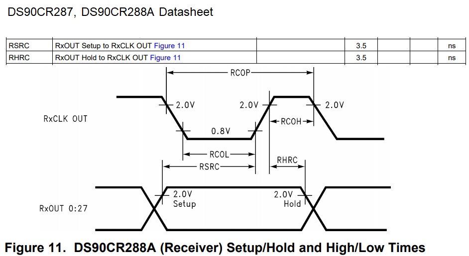
I think that the product is not output correctly. What do you think?

Depending on the device, the image may not be displayed correctly.

Best Regards,
Ishiwata

  • Ishiwata-san

          It looks like there is 'persistence' in the Data that was captured , in other words excessive jitter since multiple cycles of data is being looked. CR288A is a source synchronous LVCMOS output device so, please capture the data by triggering on the output clock , so that there is no relative jitter between clock and data. Then measure the setup/hole time

    Thanks

    Vijay

  • Hi Vijay-san

    Thank you for your answer.Sorry for the late contact.

    Does that mean that you get a single waveform with an oscilloscope?
    Normally, when acquiring the waveform of an LVCMOS signal, it is common to integrate the waveform in a certain amount of time. What do you think?

    Jitter occurs in the distance and route environment to the oscilloscope. However, even considering Jitter, the setup time is close to 3.5nsec. I think there is almost no margin.
    Can you give us some thoughts about it?

    Best Regards,
    Ishiwata

  • Ishiwata-san

        This is correct. You need to use single clock waveform on the oscilloscope. Please note that in a source-synchronous system, the current clock waveform samples the current data. So jitter accumulation on the clock/data will not affect the sampling

    Thanks

    Vijay

  • Vijaya-san,

    Please allow me to get into this communication path.

    As you advised, the screen shot was taken triggered with CMOS output clock.
    It is true that the screen shot was done in persistent mode.

    I suspect that the DS90CR288 samples input LVDS signal using recovered clock inside
    the IC and output LVCMOS data.
    The recovered clock is output as the CMOS clock.
    So, the transition timing between the CMOS data and the CMOS Clock should be consistent.
    Another wards, DS90CR288 determines the transition timing delta between the CMOS data
    and the CMOS Clock.

    Focusing on the CMOS clock, you do not see any remarkable jitter.
    However, there are substantial jitter on CMOS data.
    It means that something in DS90CR288 may case this jitter and eats timing margin specified on
    the datasheet.
    Each time CMOS data are output, this transition timing is validated.
    The persistence mode can make it cleared. If you take screen shot many times, you can
    capture such instance.  The persistent mode makes it easier.

    Mita

  • Mita-san

         Each CMOS data is independently clocked by CMOS clock so the setup/hole is determined only by that edge. It does not matter how much there is on the clock or on the data. All that matters is see if there is any relative jitter between clock and data in a source synchronous system in a cycle-cycle fashion. I dont see that issue here

    Thanks

    Vijay

  • Vijayi-san,

    Thank you for your response and sorry for the delay of my response.

    Please re-focus on the set up and hold time of the device.

    Do you agree that DS90CR288A determines the setup time and hold time?
    If so, the jitter between CLOCK and Data is originated by the DS90CR288A.


    In addition, the setup time shod not be bellower than 3.5 ns which is specified
    On the datasheet.
    If the setup time is less than 3.5 ns, doe it means that something occurs in
    DS90CR288A?

    Mita

  • Hello Mita-san

        Setup/hold time need to be measured by triggering on clock edge and looking at how far the corresponding data edge is from the triggered clock edge. From the waveform shown above, it shows that the scope is not triggering on the clock, so the setup/hold time you are measuring is being measured with respect to the current edge of clock and a data edge that was captured several cycles before which is why the measurement is incorrect.. Also setup/hold time for these devices are specified at the pins of the device. So if the data is collected at the edge of a PCB trace which can add skew/high frequency jitter it would not be accurate. So the setup/hold time measurement must be measured without persistence mode with scope triggered on clock edge, and time delta between current edge of clock and data measured. If you have it in persistence you would be aligning a clock edge and be looking at a data edge that is lot of cycles away and in that case, accumulated jitter on the data affects your measurement result

    Thanks

    Vijay

  • Hellow Vijayi-san,

    Thank you for your answer.
    I want to exchange information with you directly by E-mail or E2E private message.

    We would like to send you detail information using E2E private message or your E-mail address directly.
    Because the circuit data contains customer's confidential contents.
    Could you accept friend request on E2E or share us your E-mail address?
    And then, we attach my E-mail address;
    My Email Address : ishiwata-s@macnica.co.jp

    Best Regards,
    Ishiwata

  • Hi Team

    I have no response.
    Or have you already sent an e-mail?

    Could you send me e-mail?

    Best Regards,
    Ishiwata

  • Ishiwata-san

         Please send me a private E2E message. You can also send me a friend request and I can accept (I had not seen a request yet!)

    Thanks

    Vijay

  • Hi Team

    There was no response to the private message.
    We received a single shot waveform from a customer. Check the waveform.
    Put the waveform here again.

    DS90CR288A does not keep the setup / hold time of LVCMOS output.
    At DS90CR288A setup is out of specs. Please tell us your opinion.

    Best Regards,
    Ishiwata

  • Ishiwata-san

          It seems you have 2 tickets open for the exact same issue. We are closing this thread and we will continue to interact in this other thread

    http://e2e.ti.com/support/interface/f/138/p/844158/3140432#3140432

    Thanks

    Vijay

  • Dear Sir,

    For one of my application I intend to use DS90CR288A & DS90CR287A between two FPGA board data transfer. My simple question is in one TX/RX clock in each LVDS line 7 bit of data is transferring. Does it requires a 7 times faster clock to retrieve these serial data to convert in parallel form. Kindly reply. Thanks.

    das.anindya2015@outlook.com

  • Das

       Yes. To recover the data internally you do need a clock that is 7x faster than the input clock

    Thanks

    Vijay