Other Parts Discussed in Thread: DS90UB953-Q1
Hello,
I would like to understand, when using DS90UB953-Q1 / DS90UB934-Q1 in backwards compatibility mode, how does DS90UB934-Q1 outputs HSYNC and VSYNC signals, since there isn' t any external HSYNC or VSYNC signal input from the DS90UB953-Q1 side.
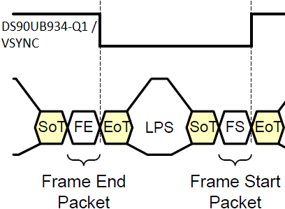
How does it exactly converting the MIPI frame into these sync signals ? The ToF sensor I am using has RAW12 output and in the CSI-2 MIPI frame, it has the Line & Frame Blank information included, so I assume it somehow calculates these blank timings and outputs them accordingly. Or does the deserializer re-constructs these control signals somehow from scratch depending on the pixel count or etc. ? I couldn' t find any timing diagrams on these, except Figure 6 & 7 on the datasheet..
So I would like to be sure that the timings will be satisfied and the interface will be compatible between DS90UB934-Q1 and μC.
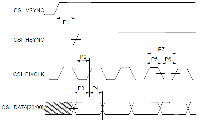
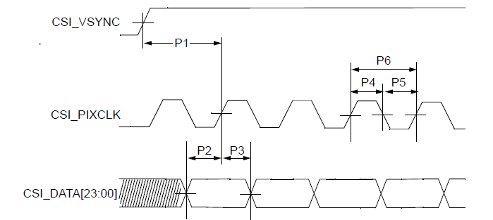
You can find the input timing requirements from my μC below:
Gated Clock Mode:
v1
v2
Ungated Clock Mode:
Thank you in advance.
Kind Regards,
Berkay Ozturk