This thread has been locked.

If you have a related question, please click the "Ask a related question" button in the top right corner. The newly created question will be automatically linked to this question.

PCA9306: PCA9306 Pull High Question

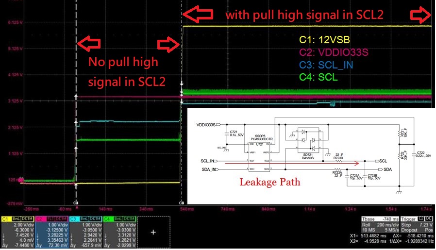
Part Number: PCA9306

We use the below circuit for the PCA9306 design. We find when the SCL1 provide the signal input, then the output signal just only half of Vref, 1.5V. When we pull high a 3.3V with series 50k resistor at SCL2 bus. Then the SCL2 signal can turn to high as same Vref. May I know the SDA/SCL bus need to pull high voltage or not? Why?

BR,

Gary

  • Gary,

    The PCA9306 is designed to conduct low levels but be high-impedance to high levels.  This behavior allows it to function as a translator between two different voltage domains.  It does mean that a pull-up resistance is required on both sides of the device, though.  For more details on this, you may want to reference Section 8.1.2 of the datasheet.  Please let me know if this isn't clear.

    Are you able to add the pull-up resistance to your design?

    I also noticed that EN is tied to a voltage divider in your schematic.  For proper functionality, we typically recommend tying EN and VREF2 together and then pulling them high via a 200-kOhm resistance.  Did you have a particular reason for using the device in this way?

    Regards,
    Max

  • Hi Max,

    Thanks for your support.

    May I know what is the internal design for the SDA/SCL? It's a BJT or FET. My customer want to know why the SCL voltage just only half of VCC before external pull high voltage ready? What reason cause the SCL only half of VCC? Thanks.

    BR,

    Gary

  • Hi Gary,

    You can refer to Figure 6 in the datasheet to better understand how the VREF inputs are used in order to establish the internal voltage that is used as a threshold for whether the SDA/SCL switches will conduct.  With the customer's set-up, the EN signal is being forced to a voltage (by the external divider circuit) rather than regulating to VREF1 + Vth.  (The design is FET based, so Vth is about 0.6 V.)  This means that instead of stopping conduction when the voltage at either side is near VREF1, it will instead stop conducting when the voltage is at VEN - Vth.  I believe this is why you are seeing the lower voltages on SDA/SCL.

    I'd recommend changing the connections to either match Figure 10 or Figure 11 in the datasheet.  Let me know if this is unclear or if you have any further questions.

    Regards,
    Max