This thread has been locked.

If you have a related question, please click the "Ask a related question" button in the top right corner. The newly created question will be automatically linked to this question.

DP83867IR: RGMII timing questions

Part Number: DP83867IR

Hello,

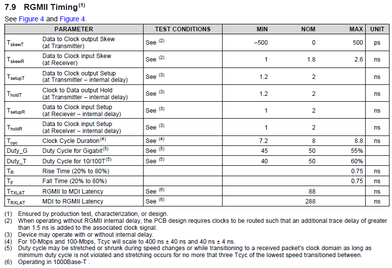
my customer is currently doing a design with the DP83867IR and he has a couple of open questions regarding the RGMII Timing diagrams and figures below:


Why are two different values for transmitters / receivers given here?

Who is the transmitter or receiver? (the customer would have assumed that one of them would have to be their FPGA, but then the question arises as to why TI assumes a timing for the routing path between the transmitter / receiver, but that can not be known at all).

The engineer has currently configured the PHY to internally delay the clock on the Rx side. On the Tx side, the delay is ensured by the FPGA (no delay in the PHY).

Which Setup / Hold values for the Rx signals directly at the output of the PHY can he expect? Which setup / hold values does he have to guarantee at the PHY input for the TX values?

regards,

Stani

  • Hi Stani,

    The RX pins of the PHY are actually output of the PHY connected to input of the FPGA. The TX pins are input to the PHY connected to the output of the FPGA. The timing parameters that relate to the output pins of the PHY are the performance metrics of the PHY showing the timing values of the RGMII signals originating from the PHY. The timing parameters related to the input pins of the PHY are the timing requirements of the PHY which need to be met in order for RGMII to work correctly. This is how it is specified in the RGMII standard so we use that in the datasheet. 

    If the application uses internal delay of the PHY then customer should check that there are no internal delays on the MAC. The delays can be due to length mismatch as well but the general practice is to keep the traces length matched and use internal delays for RGMII operation.

    -Regards

    Aniruddha

  • Hi Aniruddha,

    thanks for the prompt response and the support.

    The answers weren't clear enough for the customer so he asked if we could please confirm/correct his interpretation of the answers we provided to his questions:

    1. Why are two different values for transmitters / receivers given here?

    Because this is how it is specified in the RGMII standard and so we used it in the datasheet --> Is there an actual device specific timing that describes the concrete properties of our DP83867IR (for example, if the internal delay is enabled / disabled)? If it is said that I set an internal RxClk delay of 2 ns, I would expect the device to provide approximately 2 ns of setup / hold (and not just about 1 ns) - that would greatly relax our timing.

    2. Who is the transmitter or receiver?

    Rx pins of PHY are outputs --> Source of data (transmitter) timing is valid
    Tx pins of the PHY are inputs = receiver timing is valid

    3. Which Setup / Hold values for the Rx signals directly at the output of the PHY can he expect?

    Source of data - timing --> TsetupT / T hold T --> each 1.2 ns

    4. Which setup / hold values does he have to guarantee at the PHY input for the TX values?

    could you please derive this for me from the given data? We have deactivated the PHY internal delays for the Tx signals.

    In further investigations, we have since discovered that there are problems with impedance matching on our device.
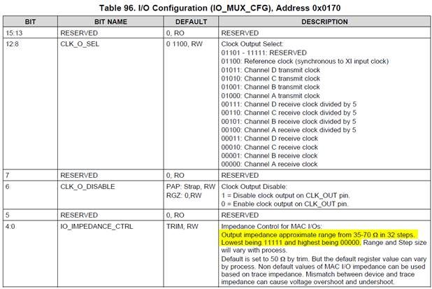
    When trying to adjust the impedance of the PHY via register 0x170 (IO_MUX_CFG, IO_IMPEDANCE_CTRL), we noticed that writing the value "11111" against the data sheet gives the highest output impedance and the value "00000" the smallest impedance:
    At the very least, writing the value "11111" will cause the signals on a 68 ohm line resistance board to have beautiful, steep edges, while writing the value "00000" (which, according to the docs, equals 70 ohms) will result in communication breaks off because the signals are so bad. Can you please clarify and confirm this?

    Best regards,

    Stani


  • Hello Aniruddha,

    is there any feedback you can share here please?

    Regards,

    Stani

  • Hello Aniruddha,

    could you please provide feedback to the questions above?

    Furthermore, the customer asked if there is an IBIS model for the PHY for 70 Ohm impedance on the RGMII signals (PHY --> FPGA)?

    Regards,

    Stani

  • Aniruddha,

    please provide an update to the questions above asap!

    Franziskus

  • Hi,

    Our Apollogies for the delayed response. We have few other priority issues to look at and causing delays in responding.

    Find my comments inline.

    Regards,
    Geet

     Why are two different values for transmitters / receivers given here?

    Because this is how it is specified in the RGMII standard and so we used it in the datasheet --> Is there an actual device specific timing that describes the concrete properties of our DP83867IR (for example, if the internal delay is enabled / disabled)? If it is said that I set an internal RxClk delay of 2 ns, I would expect the device to provide approximately 2 ns of setup / hold (and not just about 1 ns) - that would greatly relax our timing.

    The functionality of the internal delay to provide option to adjust the skew between Clock and Data. Using register 0x32 and 0x86, you shall be able to adjust the delay at accuracy of 0.25 ns

    2. Who is the transmitter or receiver?

    Rx pins of PHY are outputs --> Source of data (transmitter) timing is valid
    Tx pins of the PHY are inputs = receiver timing is valid

    3. Which Setup / Hold values for the Rx signals directly at the output of the PHY can he expect?

    Source of data - timing --> TsetupT / T hold T --> each 1.2 ns

    This is with internal delay enabled.

    4. Which setup / hold values does he have to guarantee at the PHY input for the TX values?

    could you please derive this for me from the given data? We have deactivated the PHY internal delays for the Tx signals.

    In this case, Data to clock skew is expected to be +/- 500 ps ( Item 1 in timing table).

    In further investigations, we have since discovered that there are problems with impedance matching on our device.
    When trying to adjust the impedance of the PHY via register 0x170 (IO_MUX_CFG, IO_IMPEDANCE_CTRL), we noticed that writing the value "11111" against the data sheet gives the highest output impedance and the value "00000" the smallest impedance:
    At the very least, writing the value "11111" will cause the signals on a 68 ohm line resistance board to have beautiful, steep edges, while writing the value "00000" (which, according to the docs, equals 70 ohms) will result in communication breaks off because the signals are so bad. Can you please clarify and confirm this?

    Suggest, read the default value. This is set in test to match 50 ohm. Increment this value will increase the impedance and reducing the value will reduce the impedance. 

  • HI Stani,

    Please find my replies below,

    Q1. We have a delay table in the datasheet that lists out the various settings of register 0x86 which correspond to RGMII delays. By default the delay is set to 2ns on both RX and TX lines. When the internal delays of the PHY are activated, the RMGII signals will be delayed by 2ns. It can be checked on a scope for RX signals as they are output.

    Q2 -Q4 are related to RGMII standard and its implementation in the PHY. We have an app note that goes in to these details and provides some calculation on how setup/hold times work: 

    Register 0x170 is set to correspond to 50ohm impedance. Since the board traces are set to 68ohms, it would be expected that increasing the impedance through register 0x170 should result in improved signal integrity. The observation by customer is correct. However, I must mention that the impedance value is only characterized for 50ohms. The min and max values are expected values and not characterized. 

    -Regards

    Aniruddha

  • Thanks Geet and Aniruddha!
    I will come back with customer feedback.

    Meanwhile, can you comment the remaining question about the IBIS model:
    Furthermore, the customer asked if there is an IBIS model for the PHY for 70 Ohm impedance on the RGMII signals (PHY --> FPGA)?

    Thanks!

  • Geet,

    in addition to the question about the IBIS model, there is one more thing to clarify:

    Your statement about the impedance setting is contradictory to the datasheet. I have attached the datasheet excerpt below for comparison.

    • Increment this value will increase the impedance and reducing the value will reduce the impedance.

    Can you please clarify?

    Thanks


  • Sorry for my multiple posts, but my customer came back with more questions.

    Here's a list of all open questions, including my two posts above:

    1. Post from Mon, Sep 23 2019 12:30 PM:
      1. IBIS model: the customer asked if there is an IBIS model for the PHY for 70 Ohm impedance on the RGMII signals (PHY --> FPGA)?

    2. Post from Mon, Sep 23 2019 2:23 PM:
      1. Please clarify the behavior of the IO_IMPEDANCE_CTRL bits.
        Your statement is contradictory to the datasheet. Will incrementing this value increase or decrease the impedance?
    3. New questions:
      1. In the document you referenced below (http://www.ti.com/lit/an/snla243/snla243.pdf) the following values are specified:

        I think this is, what I was searching for and what I had expected to be available in the datasheet! But still some questions on this:
        1. Are these values specific for the DP83867? I didn’t find them in the datasheet – why not?
        2. Based on these values, can I assume that the delay between RxClk and RxD directly at the PHY-Pins (with PHY-internal delay of 2 ns) is:
          2 ns +- (IDvar+IOskew) = 2ns +-0.55 ns ? (This would result in a Setup/Hold time of 1.45 ns as far as I understand)
        3. Based on these values, can I assume that the required Setup/Hold times for Tx-Signals (without PHY-internal delay) directly at the PHY-Pins have to be:
          Setup: MINsr + IOskew  =  0.5 ns + 0.35 ns = 0.85 ns
          Hold:   MINhr + IOskew  =  0.25 ns + 0.35 ns = 0.6 ns
          Can you confirm this?
      2. It would be great if you could confirm that we can use these values without getting any timing-problems regarding the PHY, as this would relax our timing a lot.

    Thanks!

  • Hello Geet, Aniruddha,

    could you please clarify the remaining questions summarised in the previous post from Franziskus?

    Regards,

    Stani 

  • Hi Stani,

    We currently only have one IBIS model, we don't have another IBIS model for 70ohms. For the impedance settings, please follow the datasheet guidance: 11111 corresponds to lower impedance and 00000 corresponds to higher impedance.

    Regarding the Table 3 values mentioned in the app note, they are design simulation values and are not characterized. That is why we publish them in an app note and not in the datasheet. As per the datasheet the MAC needs to be as per RGMII spec to meet the PHY requirement. Then we took a closer look at our design to find out that when Internal delay of the PHY is used along with close length matching on the RGMII traces we have about 0.35ns margin on the setup time and 0.2ns margin on the hold time. This also assumes that the MAC is not adding any extra internal delays. Even after that 0.35ns and 0.2ns margins are design estimates and i would recommend adding some buffer value when using these numbers for calculations.

    -Regards

    Aniruddha