This thread has been locked.

If you have a related question, please click the "Ask a related question" button in the top right corner. The newly created question will be automatically linked to this question.

SN65HVD62: OOK signal loop's attenuation

Part Number: SN65HVD62


Hi Team,

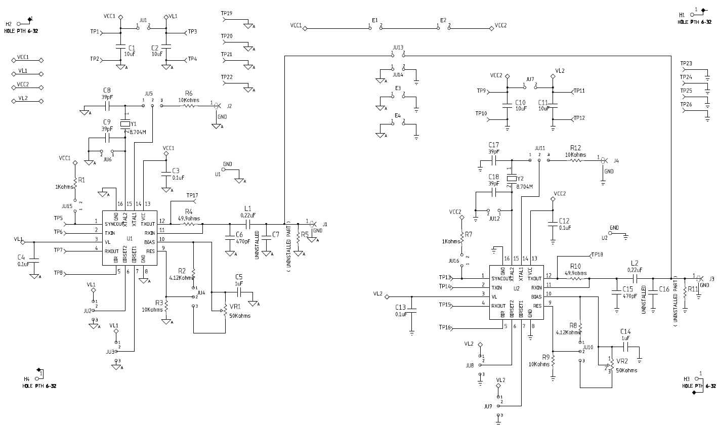
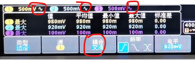
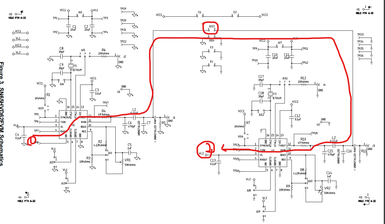
Our customer tries the OOK loop. install JU13. And input +3dB OOK signal at point 1. Test the output OOK signal at point 2.

They found the output signal amplitude is only 887mV(nearly -3dB). That is to say, after this loop, it has 6db attenuation.

Is this test result correct? If it is correct, is there any other method to optimize this attenuation?

Thanks!

BR

Marvin

  • Hi Marvin,

    Is the OOK signal injected at the TXOUT port?  It looks on your figure like it may connect to RXOUT, which wouldn't make sense (the RXOUT/TXIN pins provide the base band logic-level signals).  Can you please verify the signal amplitude at both the TXOUT side (after the RF signal is connected to the PCB) and the RXIN side (at the other end of the tranmission line)?  Do you see similar loss if you use the SN65HVD62 transmitter rather than your own source?  Are the SN65HVD62 devices powered during the test, and if so how are they configured?

    Regards,
    Max

  • Hi Max,

    I draw a wrong path. It should be TXIN-->JU13-->RXOUT.

    If so, from your experience, how much will the signal attenuate?

    Thanks!

    BR

    Marvin

  • Hi Marvin,

    That path still doesn't make sense - the TXIN and RXOUT interfaces are independent of the RF interface.  Are you sure you don't mean the signal is applied at TXOUT and measured at RXIN (i.e., at opposite ends of the RF channel)?  If that is the case, I would still be curious to know the signal amplitude measured at TXOUT, RXIN, and the mid-point (JU13).

    Regards,
    Max

  • Hi Max,

    Sorry for the wrong information. You are correct. We tried to measure the TXOUT and RXIN signal again.

    1) Install JU13. Short TP6(TXIN) and measure TP17(TXOUT), JU13 and one single-end of C15(RXIN) using the EVM board. 

    Case1.1:

    CH1: TP17(TXOUT); CH2: JU13; CH3: C15(RXIN);

    (R5 and R11 are not installed. Coax cable is not attached.)

    Case 1.2:

    CH1: C15(RXIN);

    (R5 is installed. R11 is not installed. Coax cable is not attached.)

    From the above, we can see: after installing JU13, both waveforms are nearly the same.

    2) Uninstall JU13, we can see the waveform in the below:

    Case 1.3:

    CH1: TP17(TXOUT); CH2: JU13; 

    (R5 is not installed. Coax cable is not attached.)

    Case 1.4:

    CH1: TP17(TXOUT); CH2: JU13; 

    (R5 is installed. Coax cable is not attached.)

    There are several questions:

    1) For case 1.1 and case 1.2, it seems there is no big effect whether we install the 50ohm load. 

    Can I think R10 is regarded as 50ohm load when only installing JU13? However, why is this waveform nearly the same when installing JU13 and R5? R5 and R10 should be in parallel and the equivalent load is nearly 25ohm.

    2) If uninstall  JU13, we can easily the 50ohm load makes JU13 attenuate 50% or -3dB.

    Our customer doesn't want this -3dB attenuation. And they have their own impedance matching network following 0.22uf cap.

    If so, can we remove R4(49.9ohm) and let them do their own impedance matching network for coax cable and other loads? Short TXOUT and RXIN, is it ok?

    3) If we can't remove R4(49.9ohm), is there any other method to decrease -3dB attenuation?

    -3dB attenuation is too big.

    Thanks!

    BR

    Marvin

    EVM board schematic:

  • Marvin,

    Thanks for sharing the experiments you have done on the device. We may need to solve the puzzle step by step.

    How did you measure TP17 in your test case 1.1? In general TX output has some default DC bias voltage. It looks the waveform has 0V common mode.

    Can you also check the RES resistance to make sure it's not changed?

    Back to the basic concept, SN65HVD62 is designed to drive a 50Ohm load system, which means the termination should match the cable impedance (50Ohm). If the signal integrity has to be maintained, the attenuation would be unavoidable.

    Regards,

    Hao 

  • Hi Hao,

    It seems I didn't summit the reply successfully yesterday.

    For your 1st question, our customer is using AC coupling.

    According to your saying, it is defined to drive a 50Ohm load system. Is it to say, -3dB attenuation can't be avoided? 

    If they define a impedance matching network after 0.22uf, can they remove 50ohm(R4) between TXOUT and RXIN? That to say, we don't need to care about signal integrity, especially signal reflection.

    Thanks!

    BR

    Marvin

  • Marvin,

    Thanks for pointing out the AC probe. It makes sense to me now. Yes the impedance matching network could replace 50Ohm. R4 can be considered as the output impedance of the driver. If the cable is short and reflection is negligible, you can try driving into a high impedance (like open). I personally have never done this, but it may work for your application.

    Regards,

    Hao