This thread has been locked.

If you have a related question, please click the "Ask a related question" button in the top right corner. The newly created question will be automatically linked to this question.

PCA9306: design discussion about LDO and function block

Part Number: PCA9306

Hi,

Customer has questions below, please check. Thanks.

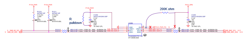
1. Do you have structure diagram for the NMOS in PCA9306? And Rds value between Vref1 and Vref2?

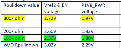
2. Design use LDO=1.8V and found the VCC1 can't regulate issue. To follow the datasheet calculate Rpulldown=300kohm{1.8/(3.3-1.8-0.6)*200K*0.75}, but VCC1 still up to 1.92v, try to  put 100kohm then the Vout=1.8V, any concern to use 100kohm?

  • Hi Lynn,

    You can see a diagram of the internal FET between VREF1 and VREF2 here:

    https://e2e.ti.com/support/interface/f/138/t/699627

    With proper connections to the device, the RDS(on) will be dynamic and set so that a bias voltage of about VREF1 + 0.6 V is present on the EN pin.  The IDS current is then VREF2 - VEN / 200 kOhm, which in this case would be 4.5 uA.

    It looks like in this schematic the VREF2 pin may be directly shorted to 3.3 V, though.  Can you please double-check this?  VREF2 should be connected to EN and both pins should be connected through a 200-kOhm resistance to the side 2 pull-up voltage.  The 200 kOhm resistance is important for limiting the current flowing through the device.

    Max

  • Hi Max,

    This is Wiwynn RD Dennis. Our original design is the VREF2 pin directly shorted to 3.3V and we measured 2.2V from VREF1 pin. But our VREF1 is connected to 1.8V LDO output.

    So we added 200k between VREF2/EN pin and 3.3V(P3V3_DPB), Lynn provided our measurement result above.

    We just want to know should we use 100K ohm Rpulldown for our application ?

    Because we already started to rework and provide the all PCBA to our customer before Wednesday.

    Please help to check if 100K pulldown resistor is available because 300K still can't meet our 1.8V criteria.

    Thanks.

  • Hi Dennis,

    Thanks for your introduction.  A 100-kOhm pull-down on VREF1 is OK to use.  As long as the 200-kOhm resistance is present on VREF2 the current flowing through the PCA9306 will be limited to safe levels.  I just wanted to make sure that your VREF2/EN connection was correct so that you do not see any other problems.

    Regards,
    Max

  • Hi Max,

    Thanks for your reply. Our VREF2 and EN pin is tied together through 200K to P3V3_DPB. After the reworked circuitry, our 1.8V power rail (VREF1) is normally output (change back to 1.8V) and we don't see any other problems now. We will let you know if any other problems happen.

  • Hi Dennis,

    I'm glad you have been able to get everything working!  If you have any issues in the future please do not hesitate to create a new thread.

    Regards,
    Max

  • Hi Max,

    During our validation test, we found P3V3 side will be low when M.2 SSD initial state at power on condition.

    So we add a 0.47uF cap between VREF2+EN and GND, same as your figure 17 of PCA9306 datasheet.

    Then we could solve this issue.

    Do you have any suggestion for this cap design because we found your datasheet 9.2.2.1 description " A 100-pF capacitor is recommend.

    Please advise if any concern for our 0.47uF design.

  • Hi Dennis,

    Larger capacitor values are fine to use.

    When the EN pin voltage ramps to a large enough level, any "low" levels on either side will cause the device to conduct.  Without the large filter capacitor, it looks like EN ramps up while the 1.8-V side is still ramping.  This causes the 3.3-V side to be pulled down.  Introducing the capacitor makes the EN ramp slow enough that the 1.8-V ramp-up can complete before the PCA9306 becomes enabled.

    Regards,
    Max