This thread has been locked.

If you have a related question, please click the "Ask a related question" button in the top right corner. The newly created question will be automatically linked to this question.

Problem reading ID ADS1298 over SPI with Raspberry pi 2 B

Other Parts Discussed in Thread: ADS1298, ADS1298ECGFE-PDK

Hello,

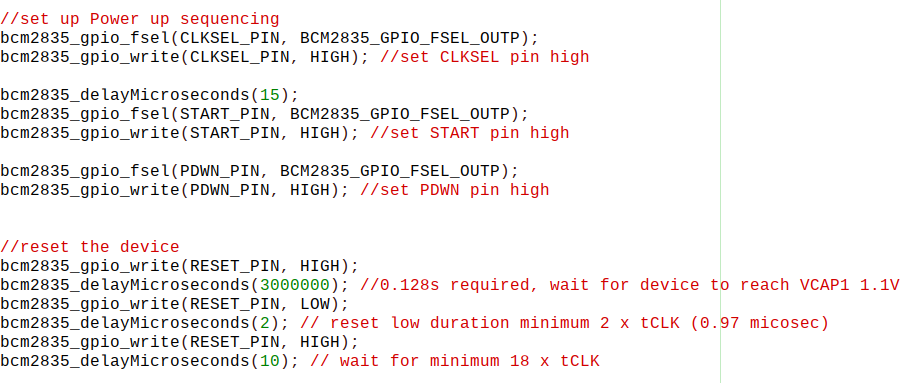
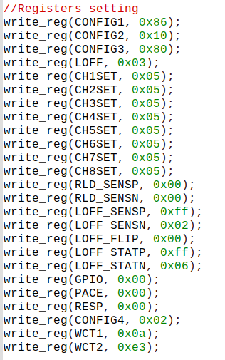
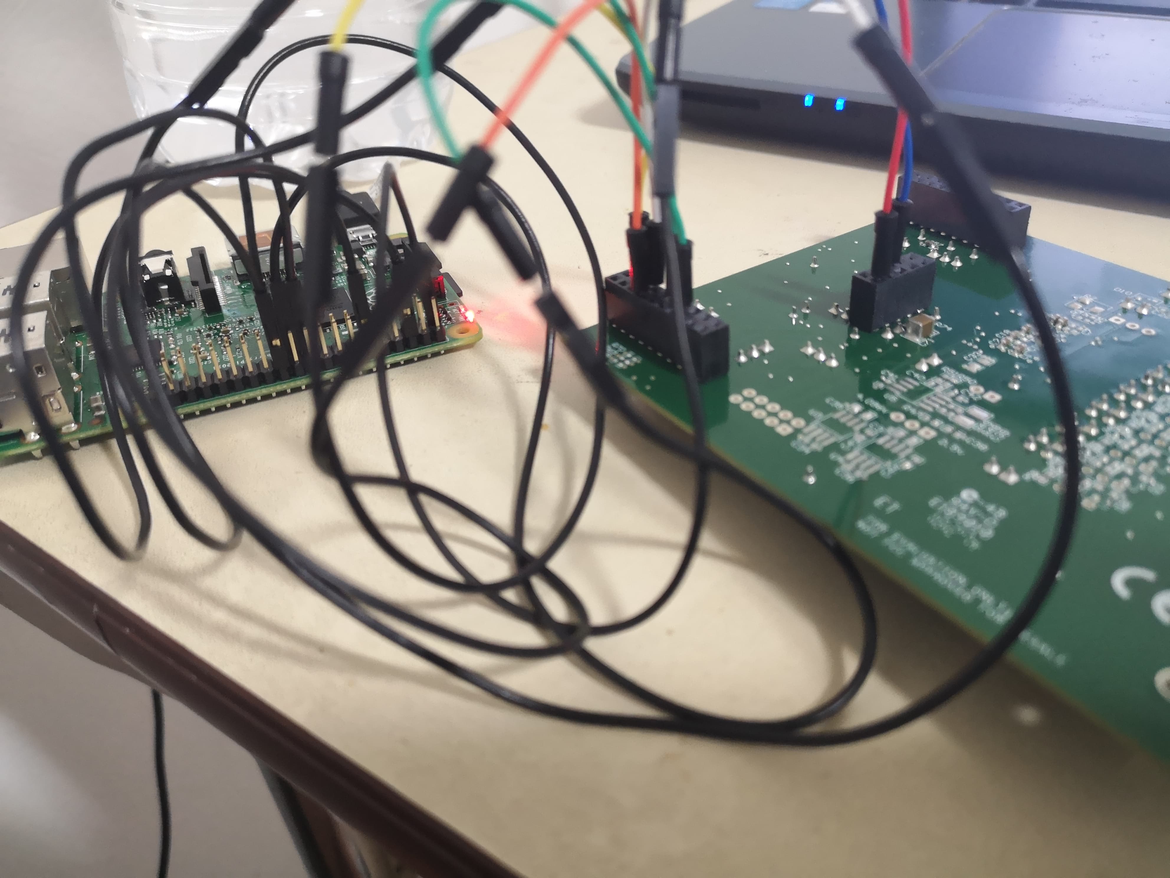
I am a newbie and recently doing my project with ADS1298 and trying as first step to power the ADS1298EVM (without MMB0) by Raspberry Pi 2 Board (I am not sure if it is possible?). Im trying to build SPI between them (ADS as Slave, Raspberry Pi as Master). But i didnt get the result that i expected when i read the ID device. My SPI connections look like this:

Raspberry                                            ADS1298EVM

    3.3V                      -----                      Pin 9 (on J4)

    GND                     -----                      Pin 6 (on J4)

   Pin 23 (SCLK)       ------                     Pin 3 (CLK) (on J3) 

   Pin 24 (CE0)         -------                    Pin 7 (CS) (on J3)

   Pin 19 (MOSI)      -------                     Pin 11 (DIN) (on J3)

   Pin 21 (MISO)       -------                     Pin 13 (DOUT) (on J3)

   Pin 12 (GPIO 18)    -------                   Pin 8 (RESETB) (on J3)   

    and here is my code ussing BCM2835 Library :

#include <fcntl.h>
#include <sys/ioctl.h>
#include <linux/spi/spidev.h>

#include <stdio.h>
#include <bcm2835.h>
#include "/home/pi/Desktop/ADS1298.h"

#define CS_PIN RPI_BPLUS_GPIO_J8_24 //CS pin CE0
#define RESET_PIN RPI_BPLUS_GPIO_J8_12 //GIPO pin 18
#define MOSI_SPI RPI_BPLUS_GPIO_J8_19 //MOSI | GPIO 10
#define MISO_SPI RPI_BPLUS_GPIO_J8_21 //MISO | GPIO 9
#define CS_DELAY 5

void cs_select()
{
bcm2835_gpio_clr(CS_PIN);
}

void cs_deselect()
{
bcm2835_gpio_set(CS_PIN);
}


int main(int argc, char **argv)
{
char buffer[3];

if(!bcm2835_init())
{
return 1;
}


bcm2835_spi_begin();

bcm2835_gpio_fsel(RESET_PIN, BCM2835_GPIO_FSEL_OUTP); //set RESET_PIN as an output
bcm2835_spi_setBitOrder(BCM2835_SPI_BIT_ORDER_MSBFIRST); //set bit Order
bcm2835_spi_chipSelect(BCM2835_SPI_CS_NONE); //do not set CS automatically

//bcm2835_gpio_fsel(MOSI_SPI, BCM2835_GPIO_FSEL_OUTP); //set MOSI_SPI as an output
//bcm2835_gpio_fsel(MISO_SPI, BCM2835_GPIO_FSEL_INPT); //set MISO_SPI as an input
bcm2835_gpio_fsel(CS_PIN, BCM2835_GPIO_FSEL_OUTP); // set CS_PIN as an output

bcm2835_spi_setClockDivider(BCM2835_SPI_CLOCK_DIVIDER_16); //1.2 MHz
bcm2835_spi_setDataMode(BCM2835_SPI_MODE1);

//reset the device
bcm2835_gpio_write(RESET_PIN, LOW);
delay(2);
bcm2835_gpio_write(RESET_PIN, HIGH);
delay(128); //0.128s required

buffer[0]=(RREG | ID);
buffer[1]=0x00;
buffer[2]=0x00;

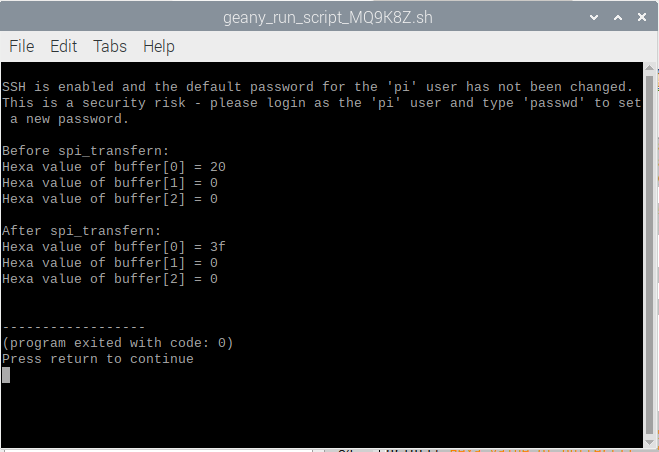
printf("Before spi_transfern:\n");
printf("Hexa value of buffer[0] = %x \n", buffer[0]);
printf("Hexa value of buffer[1] = %x \n", buffer[1]);
printf("Hexa value of buffer[2] = %x \n\n", buffer[2]);

cs_select();
bcm2835_spi_transfer(SDATAC);
bcm2835_delayMicroseconds(CS_DELAY);
cs_deselect();
bcm2835_delayMicroseconds(5);

cs_select();
bcm2835_spi_transfern(buffer,3);
bcm2835_delayMicroseconds(CS_DELAY);
cs_deselect();

printf("After spi_transfern:\n");
printf("Hexa value of buffer[0] = %x \n", buffer[0]);
printf("Hexa value of buffer[1] = %x \n", buffer[1]);
printf("Hexa value of buffer[2] = %x \n", buffer[2]);

bcm2835_spi_end();
return 0;
}

Wiring 2 device:

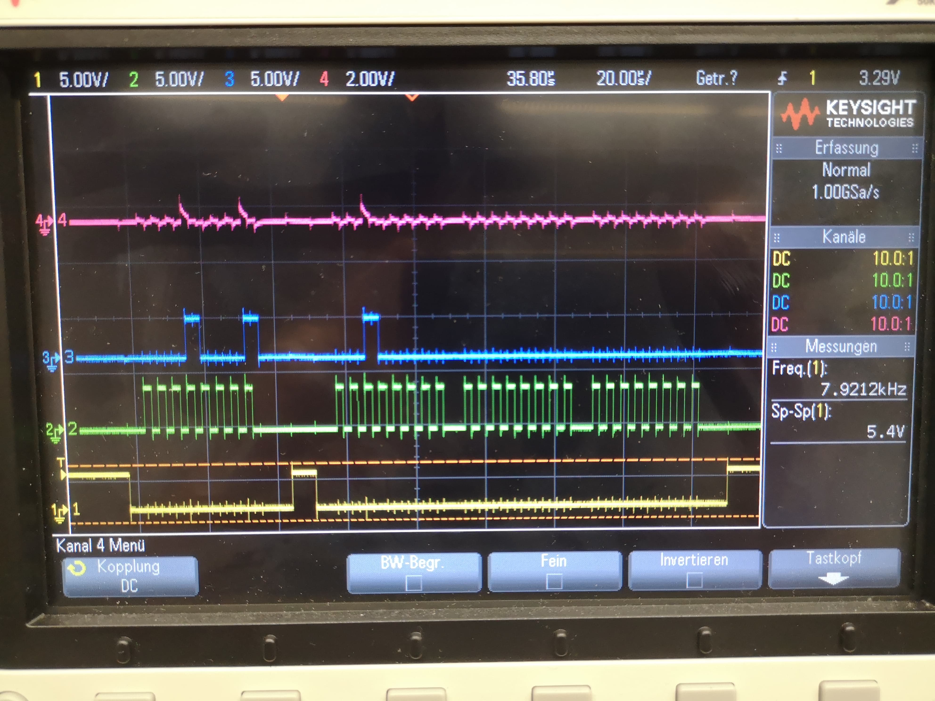
But i only get this rerult :

And then this when i took the 2 power connections out from Raspi to J4 on ADS1298: 


It seems like the value changed sometimes somehow when i connect and reconnect the 2 power wires to J4. As prove i have got this result after i put the power wires on J4 again:


  • Hi Van Tu Hoang,

    Thanks for your post and welcome to the forum! 

    The best thing to do is to consult the BIOFAQ located in my signature and the ADS1298ECGFE-PDK user's guide. 

    Make sure that the device has powered up correctly and it working functionally, then attempt to communicate using SPI. There is example code in the BIOFAQ as well. 

    Good luck! 

  • Hi Alex,

    Thank you for your quick answer.

    I have been searching for good ways for my project on this forum since months and also reading BIO-FAQ but probably couldnt be able to understand 100% what has written down.

    So my question is:  is it possible to power ADS1298EVM (without MMB0) by Raspberry Pi as i did? or do i have to definately use MMB0 to power it?

    If yes, are the connections from my Raspi on J4 correct?

  • The Raspberry Pi is not a TI device so I do not know what output power levels it is capable of. You can see the power requirements for the ADS1298 in the datasheet, and the connection diagrams for the PDK in the user's guide. 

  • Thanks for your answers again.

    I have done those steps in Figure 93 "Initial Flow at Power Up" and Figure 105 "Power-Up Timing Diagram" and still couldnt get any answers from the chip ADS1298. MOSI and CLK seem working correct. This is what i get from oscilloscope:

    Yellow - SS

    Green - SCLK

    Blue - MOSI

    Pink - MISO

    And this is a part of my code what i was following to the steps in Figure 93 and Figure 105 from Data sheet.

    By the way i see there are 2 PDWN pins on ADS1298 Board, ones on J5 and the other one on JP5. So I am actually not sure if i use the /PDWN pin correctly. I connected PDWN pin from J5 to GPIO pin on my Rasp Berry Pi.

    So is there anything that i am still missing to do? 

  • Hi Van Tu Hoang,

    One thing to consider is that the peaks of the input voltage may be exceeding the input range of the device. If you look at the 7.1 Absolute Maximum Ratings in the datasheet you will see that the digital input should not exceed DVDD/DGND by more than +/-300mV, which I think the overshoot is. Try probing the line using a spring/short ground lead close to the input signal. 

    You may need to add a small RC to these lines. Place the R next to the MCU and the C close to the ADS1298. In the neighborhood of 50ohm for the R and 10pF for the C. Let me know if this cleans up the signal.

    If you haven't done so yet, please review the timing specifications for SPI communication as well. 

  • Hi,

    To avoid this exceeding power problem i have tried to use MMB0 mother board to power the chip ADS1298 and all power supplies at test points show correct values. But it doesnt help to get ADS1298 to give any answer though. I connect DRDY pin to oscilloscope and this stays high permanent. And this is my SPI setting. My SPI SCLK Speed is 244 kHz as following:

  • Hi Van Tu Hoang,

    Please see the BIOFAQ located in my signature or search the E2E forum. Since this is being interfaced with a non TI-product I cannot offer additional support. 

  • Hi Alex,

    Thank you for responding.

    I think i have found the problem that i couldnt get any answers from the chip ADS1298. I measured VCAP1 and regconized that this voltage shows negative value (about -1,3V). I have tested at all Test Point voltages and they show correct values but VCAP1. The chip is powered by MMB0 mother board btw (trying to use ADS1298PDK with MMB0 board). So i dont know if the chip was defekt or what is the problem right now. Can you help me by telling me what it could be?  

    Van Tu, Hoang

  • Hi Van Tu, Hoang,

    What is AVSS connected to? 

  • Hi,

    Do you mean AVSS on JP20? If so, it is not connected. I am using the whole ADS1298ECG-FE Kit and only try to measure the voltages now.

    So the Ads1298 Front End is connected to MMB0 over J2, J3 and J4 as i known.

    Van Tu, Hoang

  • Hi Van Tu Hoang,

    AVSS is one of the power supply pins that the device needs to operate. The ADS1298 can either be powered from 5V on AVDD and 0V on GND & AVSS or +2.5V for AVDD, -2.5V for AVSS, and 0V connected to GND. 

    Please consult the datasheet for additional information. 

  • Hi, I have found out that i was creating a mistake on CLKSEL pin on J3. Now i am able to read device ID correctly. CLKSEL pin (J3.2) is being floating now (not connected). But i actually didnt get it really clearly. I unterstand that it must be connected to a GPIO pin on microcontroller board to be set active high
  • Hi,

    That's great to hear! 

    I think perhaps you are confusing CLKSEL and CS (Chip select). Take a look at section 9.3.2.5 Clock for more detail on CLKSEL. 

  • Hi Alex,

    Yes you're right. I am understanding it now. But right now i am facing the other problems since weeks and hope you can help me out.

    I am trying to get data from all channels from ADS1298, but when i put the electrodes on my arms or chest i didnt see anything coming out. Btw i am able to read 3 bytes status word. So what i am doing right now is using internal test signals on all channels to see if it really works with my code or my electrodes were damaged. But i cant see anything coming out either. What i understand about test signals is we dont have to use electrodes to catch the signals from the body but they will be created internal, is it correct?

    Here is my registers setting:

    Best regards

    Van Tu, Hoang

  • H Van Tu, Hoang,

    It looks like you're writing an invalid command to CONFIG3. Try changing this to xC0 from x80. 

    I would also recommend disabling all lead off features for now. 

  • Hi,

    C0 was actually the value that i set for CONFIG3 at the beginning. I have changed it all at you said but it doesnt help. Would you please like to check my code for reading 1 data right now if it is ok?

  • Unfortunately writing the code is up to the customer and changes/modifications are not supported. The example code in the BIOFAQ may help.