


VDD pins 3, 8, 15, 25, 30 - Tied to power 3.3 V with decoupling capacitor 0.1 uF.
EQ0 - EQ3 pins 11, 12, 39, 40 - Ground.
PE0 - PE3 pins 18, 19, 20, 31 - Ground.
PWDN# pin 38 - Tied to power 3.3 V without any pull up.
PWDN0# - PWDN3# pins 32, 33, 34, 35 - Tied to power 3.3 V without any pull up.
LOS0# - LOS3# pins 13, 14, 36, 37 - Not connected as no output acknowledgement feature demanded in our case.
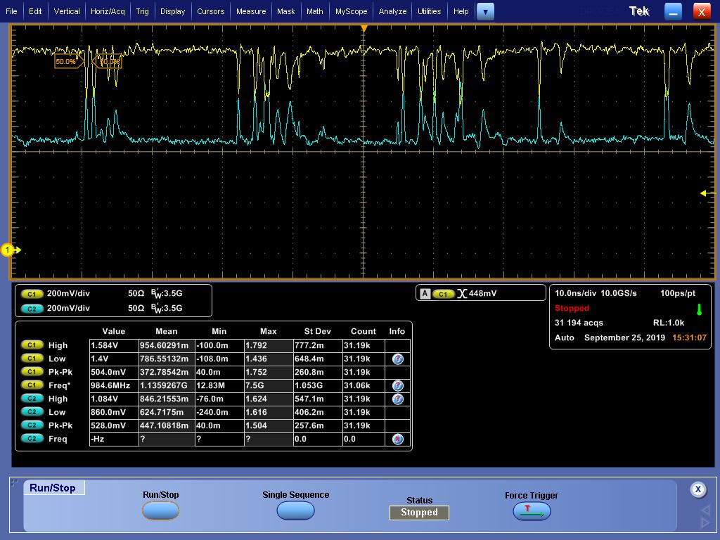
IN0 - IN4 - All LVDS inputs.
OUT0 - OUT4 - All LVDS outputs.
We observed that if all IN0 - IN4 LVDS inputs are all 0 V (no signals), OUT0 - OUT4 output channels will have behaviours as below:
a.) OUT0+ 1.3 V flat, OUT0- 1.1 V flat.
b.) OUT1+ and OUT1- both 1.2 V flat.
c.) OUT2+ 1.1 V flat, OUT2- 1.3 V flat (polarity inversion compared to item a.)).
d.) OUT3+ 1.5 V flat, OUT3- 0.9 V flat (larger peak-peak compared to item a.)).
Why the 4 output channels behaviour will be different among each other?
We try to setup the above 4 conditions to be connected to IN0 - IN4 this time, and the observations as below:
a.) If any IN+ and IN- have both 1.2 V flat (common), OUT+ and OUT- on that particular channel will surely have signals flipping.
b.) If any IN+ and IN- in LVDS differential form, OUT+ and OUT- on that particular channel will follow what the input be.
c.) Channel 2 will always have polarity inversion.
d.) All channels output peak-peak value will increase. OUT+ 1.5 V, OUT- 0.9 V.
Why common 1.2 V signals will cause signal flipping? Why channel 2 always have polarity inversion?
