


Part Number: DS80PCI402
Hello team,
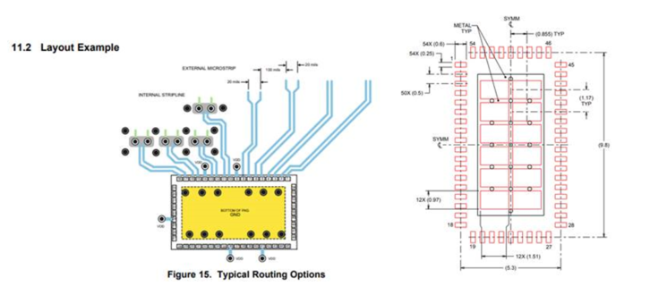
My customer was looking at part DS80PCI402 to use in a new application, and noticed that there is a discrepancy in the suggested thermal via layout. The attached footprint shows 17 vias between the solderpaste, but the layout guidelines and example show only 6 vias placed around the edge of the ground pad.
Which thermal via layout is more correct?
Thanks!
Errol
