This thread has been locked.

If you have a related question, please click the "Ask a related question" button in the top right corner. The newly created question will be automatically linked to this question.

TPS65987DDJ: TPS65987 Application issue

Part Number: TPS65987DDJ
Other Parts Discussed in Thread: TPS65987

Hi Sir,

Our customer used the TPS65987 for PC Host application,
But have some question need you help to Clarify,

Q1, If PP_CABLE & VIN_3V3 no power, then VBUS have power from PP_HV1?

Q2. Can we use TPS6598x configuration tool to setting the GPIO12 output TPS65987(Host)=High & TPS65987(Device)=Low?
Q2-1, Insert the Adapter, which one of the GPIO12 and PP_HV operates first?
Q2-2, If TPS65987 is setting Device, which one of the GPIO12 and PP_HV operates first?

Q3, In the idle state, PP_CABLE=5V, PP_HV=5V, VIN_3V3=3.3V, Does the VBUS pin of TPS65987 have output?

Q4, We are reference TPS65987EVM Design for HRESET pin setting, need to pull High Signal to TPS65987? Does the current practice have an impact on chip stability?

Q5, If Adapter is 19V, Is it configured to output 19V through FW? Not adaptive through CC?

Q6, PP_CABLE and VIN_3V3 are powerless in the shutdown state.
If the TPS65987 chip works abnormally, is there any problem with the shutdown charging?

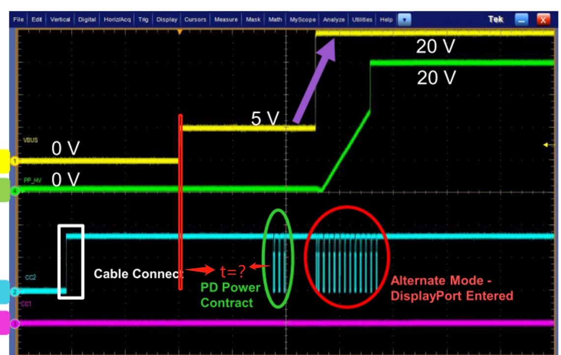
Q7, What is the T value as below?

Hugo

  • Hi Hugo,

    1. If there is no power on VIN_3V3, then the PD will attempt to get power from VBUS1 or VBUS2 which will then enable the internal LDOs for power. We have a specific application note for more details on this here: https://www.ti.com/lit/an/slvae65/slvae65.pdf

    2. Yes you can use the Configuration GUI tool to set the GPIO output and tie an event if needed. I'm not sure I understand what your secondary questions are but all of the GPIO events and functionality are explained and can be seen in the Technical Reference Manual for the PD controller: https://www.ti.com/lit/ug/slvubh2b/slvubh2b.pdf as well as the GPIO events application note: https://www.ti.com/lit/an/slvae11/slvae11.pdf 

    3. As far as the VBUS voltage, this will depend on the functionality of the device, if it is operating as a sink or source, or if the device is in a dead battery condition, etc.

    4. The schematic that you see on the TPS65987EVM design is our current up to date and working design for that device's EVM. I recommend following the requirements and considerations on the datasheet as well as the EVM user's guide.

    5. If the PD controller is designed to be a source adapter and output 19V, then the voltage will be seen on the VBUS pins if the power is being supplied to another PD controller that accepts that source capability. You won't be able to see the 19V on the CC pins because those pins are for the communication between the two PD controllers, not for power delivery purposes.

    6. I'm not sure I fully understand your question. If there is no power being provided to the PD controller, it will attempt to boot up using the VBUS pnis, assuming there is voltage there. In this "dead battery" state, the functionality will depend on how the ADCIN1 and the SPI_MISO pins are configured.

    7. I'm not sure which time interval you are referring to, however, you can reference section 6 of the datasheet for the provided timing values here: https://www.ti.com/lit/ds/symlink/tps65987d.pdf

    Thank you,

    Hari