A related question is a question created from another question. When the related question is created, it will be automatically linked to the original question.
If you have a related question, please click the "Ask a related question" button in the top right corner. The newly created question will be automatically linked to this question.
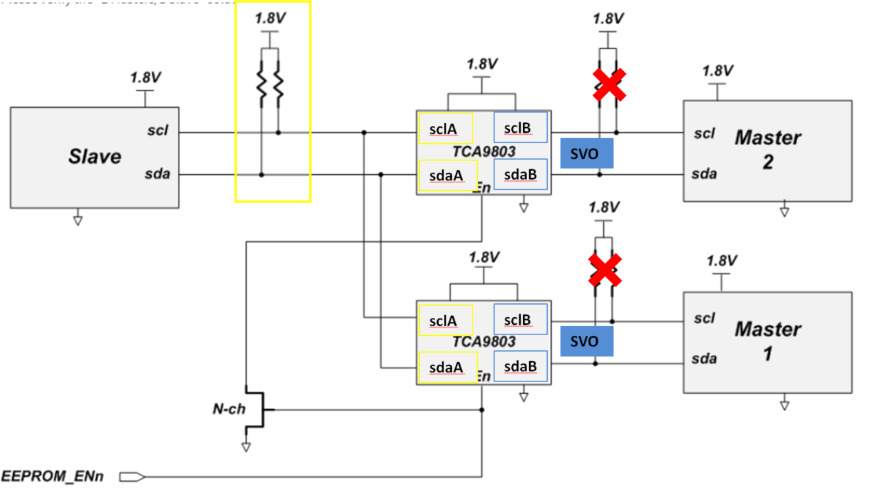
TCA9803 uses a Static Voltage Offset (SVO) on the B side of the device which does not allow it to be connected in this way:
In this case the devices can be flipped so that sclB and sdaB are on the master side (and pull-ups moved accordingly). This will avoid connecting the SVO B-sides together (A sides do not have SVO and therefore can be connected). See Figure 31 on the datasheet.
Let me know if you have any other questions and if you'd like a review of an updated schematic.
The schematic above has the B-sides of the TCA9803 sharing a common bus. This is an example of two Static Voltage Offsets sharing a bus. This is not allowed. SVOs are used by these buffers to determine from which direction a LOW is being driven. If two SVOs are present on the bus, it could cause the devices to lock-up and stop all communication on the bus. Even when the TCA9803 is disabled, (EN = GND), the SVO still remains.
To solve this, I recommended flipping the devices so that the B-side with SVO faces the Master devices and the A-sides share the common bus with the slave. Since the A-side does not have a SVO, this configuration would be allowed. In this configuration, be sure that Vol of sclB/sdaB of TCA9803 is below Vil of the Master device.
Concerning Enable times, Section 7.7 in the datasheet specifies the enable and disable times for the device. Without taking into account the propagation delay added by the FET in the schismatic (assuming ENs are toggled at the same time), there is a potential time of around 2us in which both devices would be active. On a bus operating at 400kHz, this could see a bit or two in which both masters are trying to drive the bus. During this time, glitches could be expected if both Masters are trying to drive the bus during a transition.
Let me know if this explanation makes sense or if I can clarify further.