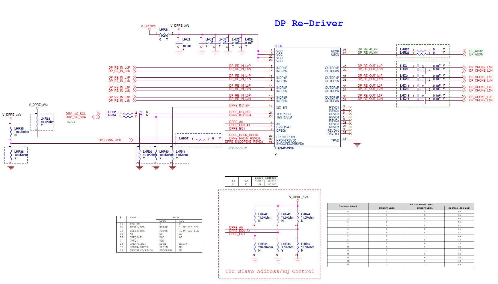
This thread has been locked.

If you have a related question, please click the "Ask a related question" button in the top right corner. The newly created question will be automatically linked to this question.

TDP142: output signal swing level

Part Number: TDP142

Hi, 

My customer is having below issue: 

Customer found the output signal swing level unbalance between Lane 0/3 and Lane1/2 when we want to check the eye diagram.

Base on this, we measured the TDP142 DP input and output.

From the measurement, the input signal swing level are the same.

But after TDP142, the output signal (Lane 0/3) swing level is attenuated, but Lane 1/2 not.

We test 2 PCBs and the symptom are the same no matter I2C or GPIO mode and Snoop enable or disable.

So, please help to check with your team is it known issue or some setting wrong.

Below the 2 PCBs setting we used.


PCB1: I2C mode, register value

Reg addr

Value

Value in binary

0x0A

0x12

0001 0010

0x10

0x88

1000 1000

0x11

0x88

1000 1000

0x12

0x00

0000 0000

0x13

0x00

0000 0000


PCB2: GPIO mode

I2C_EN (Pin17) = L (1K pull down)

SCL (pin21) = L (10K pull down)

SDA (pin22) = L (10K pull down)

A0 (pin11) = Float

DPEQ0 (pin14) = L (1K pull down)

DPEQ1 (pin2) = Float

DPEN (pin23) = H (10K pull to Vcc)

SNOOPENZ (pin29) = L (10K pull down)


Measurement waveform

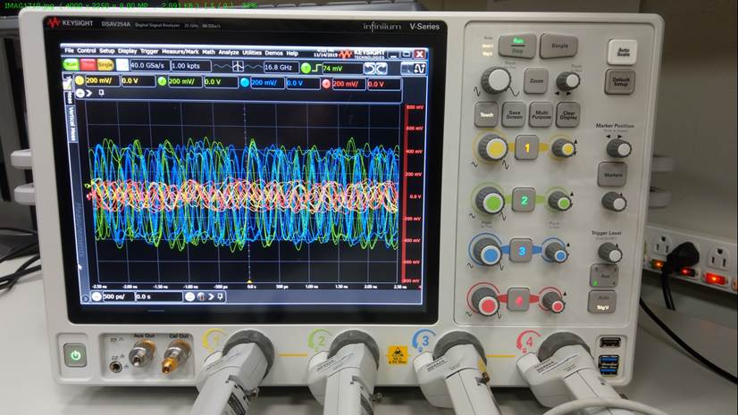
1st measurement for eye check, TDP142 output (PCB1 I2C mode)

CH1: Lane0, CH2: Lane1, CH3: Lane2, CH4: Lane3

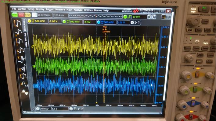
2-1 measurement, Check TDP142 input (PCB2 GPIO mode)

CH1: Lane0, CH2: Lane1, CH3: Lane2

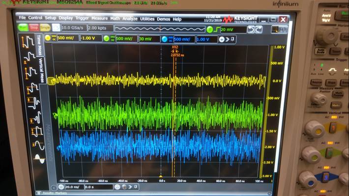
2-2 measurement, Check TDP142 output (PCB2 GPIO mode)

CH1: Lane0, CH2: Lane1, CH3: Lane2

Please let us know if you have further comments on this issue or let us know if more information needed. 

Thanks a lot for your help. 

  • Would you please try the following experiments? Would you please send me the schematic and layout for review?

    1. Please swap the scope probe between Lane 0/3 and Lane1/2 to make sure it is not probe/probe setting issue.

    2. Replace the AC coupling capacitors on Lane 0/3 

    3. X-ray DP142, does it have a solid thermal pad connection to GND? If necessary, please re-flow DP142.

    Thanks

    David

  • Hi~David:

    Schematic as attachment and reply your suggestion as below --

    1. I have swapped the probe, same symptom.

    2. Actually, I measured 2 point for TDP142 output (before and after AC cap), same symptom.

    3. I will try the X-ray.

    Schematic--

    Thanks

    Dodge

  • Dodge

    Do you have AC coupling caps on the DP142 input? 

    How does AUX being connected between the source and the sink? 

    Otherwise, the schematic looks ok.

    Thanks

    David

  • Hi~David:

    Since the source is USB/DP combo PHY (type-C), so the DP lane 0/3 is also USB RX1/RX2 path.

    And there are no AC caps on these two path.

    Just try to add cap, the swing level is same as lane 1/2 and DP work normally.

    Thanks for your feedback and support.

    Dodge

  • Hi~David:

    Even we know the root cause already but I'm curious that input AC coupling cap impact so much for TDP142 output.

    From waveform of lane 0 input signal (w/o input AC cap) that swing level is same as lane1/2 (w/ input AC cap).

    But lane 0 output signal can be attenuated to ~2/5.

    Would you please let us know why TDP142 so sensitive for input AC coupling cap?

    Thanks!!

    Dodge

  • Dodge

    1. TDP142 is a linear re-driver. So as long as the input signal amplitude is within the linear region of TDP142, the output signal will have the same amplitude as the input without compression.

    2. On the input side, when the AC coupling capacitor is present, the AC coupling capacitor changes the DC component (common-mode voltage), while passing along the AC component (voltage swing) of the signal. The internal termination of the DP142 and USB/DP combo PHY then provides the proper DC bias of the AC coupling capacitor. But without the AC coupling capacitors (DC coupled), then the internal termination will impact the voltage swing of the signal.

    Thanks

    David

  • Hi~David:

    Got it, thanks.

    Dodge

  • Hi~David:

    Another questions 

    1. TDP142 is a linear re-driver. So as long as the input signal amplitude is within the linear region of TDP142, the output signal will have the same amplitude as the input without compression.

    Q1: What's signal amplitude? DC or AC component

    Q2: What's the linear region range? Can we see that range listed in datasheet?  Is the parameter VIC (Input common mode voltage) = 0 ~ 2V  that listed in datasheet page 7 ?

    Q3: If input over the linear region, why not to keep max input for output but go compression ?

    Thanks!!

    Dodge

  • Dodge

    Please refer to Figure 2, DisplayPort Linearity Curve in the TDP142 datasheet.

    Take for example EQ0 linearity curve, when input differential voltage is 1V, the output differential voltage is also 1V. But as you go higher on the curve, you can see the output differential voltage is smaller than the input differential voltage, this is where the compression happens.

    Thanks

    David

  • Hi~David:

    But you can see my original waveform for Lane0, the input differential voltage is around 1V(p-p) but output is compressed already?

    That different with the linearity curves.

    CH1=Lane0, Input, (EQ=15, w/o input AC cap), V(p-p) ~ 1V

    CH1=Lane0, Output, V(p-p) ~250mV

    Thanks

    Dodge

  • Dodge

    Please see my previous response. The majority of reduction in signal amplitude comes from the missing AC caps, not because the linearity compression.

    2. On the input side, when the AC coupling capacitor is present, the AC coupling capacitor changes the DC component (common-mode voltage), while passing along the AC component (voltage swing) of the signal. The internal termination of the DP142 and USB/DP combo PHY then provides the proper DC bias of the AC coupling capacitor. But without the AC coupling capacitors (DC coupled), then the internal termination will impact the voltage swing of the signal.

    Thanks

    David

  • Hi~David

    Could you let us know if there is no input AC cap that will not meet or over which parameter of DC or AC Electrical Characteristics in datasheet to cause this amplitude reduction?

    Thanks!!

    Dodge

  • Dodge

    The characterization data in the datasheet assumes the input is AC-coupled per the DisplayPort spec, it does not list the condition when the input is DC-coupled as it will be a spec violation.

    Thanks

    David