This thread has been locked.

If you have a related question, please click the "Ask a related question" button in the top right corner. The newly created question will be automatically linked to this question.

PCA9306: PCA9306 used as switch with VREF2 to GPIO

Part Number:

Hi, we are using a PCA9306 as described in http://www.ti.com/lit/ds/symlink/pca9306.pdf Figure 17.
However, we have the same voltage on VREF1 and VREF2 (1.8V).
So VREF1=1.8V, VREF2&EN=200K to 1.8V GPIO.

1. What difference should we expect, compared to the suggested design in Figure 10?
In that design only EN is connected to a GPIO, and not via the 200K resistor.
VREF2 would still be connected to 1.8V via a 200K resistor.

Since neither solution fulfils the design requirements (9.2.1) I assume we will have slightly worse performance in switch mode compared to translation mode?
"The SCL switch conducts if EN is ≥0.6 V higher than SCL1 or SCL2. The same is true of SDA." (8.4)
Is suppose this means that regardless of whether we use the Figure 17 or Figure 10 design, SCL# will only be driven if the other side SCL# drops below 1.2V?

2. We also found an issue where EN is not pulled to 0V, but may stay at about 0.2V.
Since SDA #and SCL# need to be below 0.2 - 0.6V = -0.4V, can we be sure that SCL is still HI-Z, even if one SCL#/SDA# pin is at 0V?

3. Also, this alternate use-case is missing from the Q1 device data sheet.
http://www.ti.com/lit/ds/symlink/pca9306-q1.pdf

  • Hey Anders,

    Anders Kagerin said:

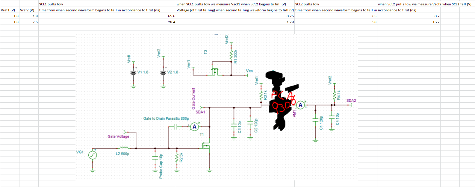
    Part Number: PCA9306

    Hi, we are using a PCA9306 as described in http://www.ti.com/lit/ds/symlink/pca9306.pdf Figure 17.
    However, we have the same voltage on VREF1 and VREF2 (1.8V).
    So VREF1=1.8V, VREF2&EN=200K to 1.8V GPIO.

    1. What difference should we expect, compared to the suggested design in Figure 10?
    In that design only EN is connected to a GPIO, and not via the 200K resistor.
    VREF2 would still be connected to 1.8V via a 200K resistor.

    Figure 10 assumes you are using Vref1=Vref2. If you are using Vref1=Vref2 but instead as figure 17 points out then I would expect the same results. The only real difference is that it would take you alittle bit longer to actually enable and disable the device because the 200k resistor is acting as the R in the RC constant which is kinda large. Otherwise you should be fine.

    Since neither solution fulfils the design requirements (9.2.1) I assume we will have slightly worse performance in switch mode compared to translation mode?

    Design requirement 9.2.1 is as you pointed out. The biasing on the enable pin which is referenced by other circuitry inside the device would be lower. This would mean you need to drive below ~1.2V, in your case, before the 'output' follows the input. If Vref2>Vref1 by ~0.6V then you would only need to drive a little below 1.8V to see the output follow the input.
    "The SCL switch conducts if EN is ≥0.6 V higher than SCL1 or SCL2. The same is true of SDA." (8.4)
    Is suppose this means that regardless of whether we use the Figure 17 or Figure 10 design, SCL# will only be driven if the other side SCL# drops below 1.2V?

    Correct.

    2. We also found an issue where EN is not pulled to 0V, but may stay at about 0.2V.

    Is there anything else connected to the EN or Vref2? This is a bit unusual.
    Since SDA #and SCL# need to be below 0.2 - 0.6V = -0.4V, can we be sure that SCL is still HI-Z, even if one SCL#/SDA# pin is at 0V?

    You are expecting the SDA/SCL pins on either side of the bus to sit at GND or below it at any point in time? If enable is below ~0.6V then the path between side 1 and side 2 of SDA/SCL should be high impedance.

    3. Also, this alternate use-case is missing from the Q1 device data sheet.
    http://www.ti.com/lit/ds/symlink/pca9306-q1.pdf

    I tried to add these new sections in a while back but ran into an issue (the issue is just approval from higher ups since people don't like it when automotive datasheets get changed without being checked off!)

    -Bobby

  • Hi Bobby,

    1. Great, slower enable times are not an issue.

    2. Yes, the GPIO starts as tristate with pull-up (40k) and we have an external pull-down of 4.68k (iirc). This is the default-power on state, which must be EN = off. When software starts we can drive the GPIO to 1.8V or 0V.

    3. Ah, bureaucracy :-)

    Thanks Bobby!

    /Anders

  • Another hypothetical question; if we would drive VREF2 & EN with a 2.5 or 3.3V GPIO, would this provide lower activation threshold?

    So VREF1 = 1.8V.
    SCL1 & SDA1 = Pull-up to 1.8V or driven to GND

    VREF2 & EN = 200K to 3.3V
    SCL2 & SDA2 = Pull-up to 1.8V or driven to GND

    I assume that SCL1 & SDA1 do not conduct until slightly below 1.8V (but higher than 1.2V), and that the same should be true for SCL2 and SDA2?
    But it also feels like there is something here that I might be missing.

    /Anders

  • Hey Anders,

    Anders Kagerin said:

    Another hypothetical question; if we would drive VREF2 & EN with a 2.5 or 3.3V GPIO, would this provide lower activation threshold?

    Similar to figure 17 where your GPIO or bias voltage is applied after the 200k resistor? If so then yes.

    So VREF1 = 1.8V.
    SCL1 & SDA1 = Pull-up to 1.8V or driven to GND

    VREF2 & EN = 200K to 3.3V
    SCL2 & SDA2 = Pull-up to 1.8V or driven to GND

    This set up would apply a voltage of around 2.4V directly to the EN to establish a higher reference voltage (the reason why we suggest user's to tie enable and Vref2 together). A simplified internal drawing is shown in figure 6 which when you tie a FET's gate and drain together, you essentially have just a PN junction AKA a diode.

    I assume that SCL1 & SDA1 do not conduct until slightly below 1.8V (but higher than 1.2V), and that the same should be true for SCL2 and SDA2?
    But it also feels like there is something here that I might be missing.

    No, I think you hit all the spots here. I did some measurements on the prop delay differences a while back and found that the differences when the reference voltage (voltage at enable) was the same as side1 and side 2 (like a switch configuration) versus the translator configuration were pretty low. Prop delays differences were around 100ns apart.

    /Anders

    Here's measurements I took from the lab on prop delays between the EN voltage at 1.8V =Vref1=Vref2 and enable voltage at ~2.5V at Vref1=1.8V and Vref2=2.5V:

    You can see the voltages I recorded of when they start to pull low. I also made my own definition for prop delay (datasheet uses 50% of Vcc but I don't like how that is defined; instead I want to know when I pull low, how long before the other side begins to pull low).

    When side 1 and side 2 have the same voltage, the prop delay times are nearly identical. If you apply 2.5V at the reference voltage (enable pin) and pull from a 1.8V rail then the prop delay is then lower, at 28.4ns as opposed to 65ns. The voltage point at which the output follows the input changes from 0.7V to 1.2V though I'm sure if I had a slower ramp down I would see these numbers be a little higher since the switches have some double digit nanosecond range for them to turn on fully.

    -Bobby

  • Awesome feedback Bobby, I greatly appreciate it!

    Best regards,
    Anders