This thread has been locked.

If you have a related question, please click the "Ask a related question" button in the top right corner. The newly created question will be automatically linked to this question.

DS90UB914A-Q1:I2C communication with S90UB953-Q1 and DS90UB914A-Q1

Part Number: DS90UB914A-Q1
Other Parts Discussed in Thread: DS90UB953-Q1EVM, ALP

We can't  I2C communication with S90UB953-Q1  and DS90UB914A-Q1.

Master device is my I2C host controller.  

  [a:sensor]  <I2C >  [b:953]  <I2C>  [c:914]  <I2C>  [d:I2C Host Controller]

    slave address

        a:sensor = 0x42

        b:953 = 0x30 (maybe I thnk 0x30 is default slave address??)

        c:914 = 0x60 

We tried following steps.

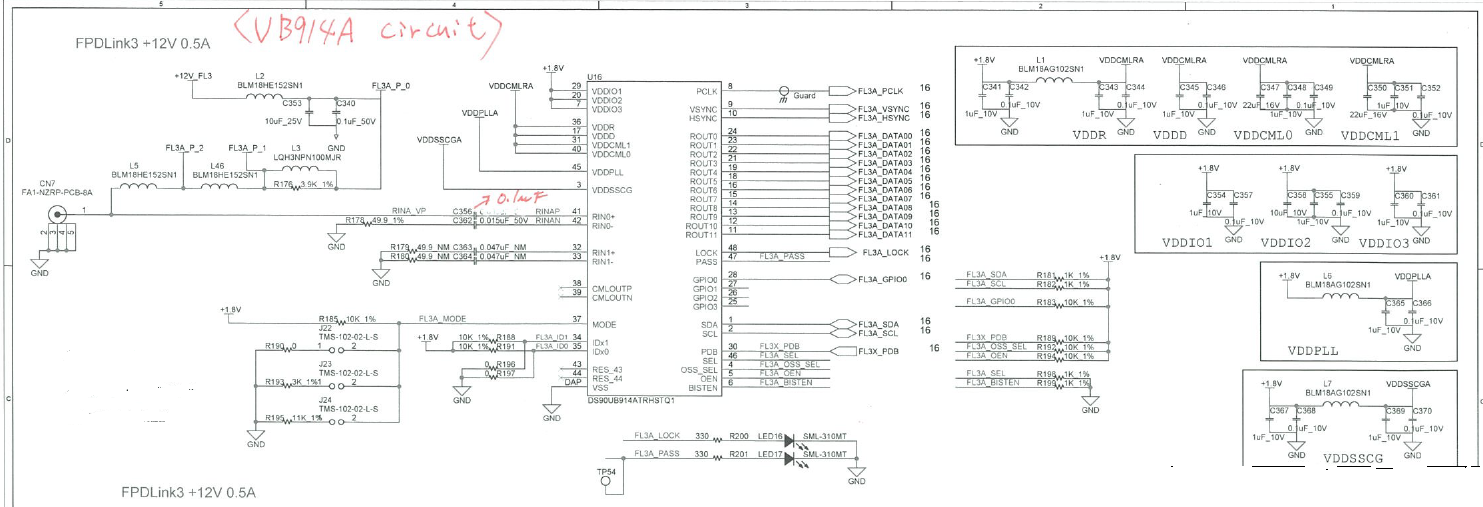
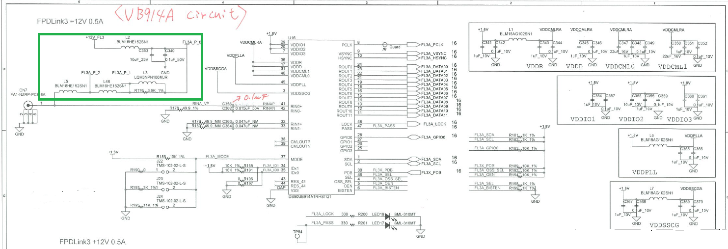
step1) The 953 MODE pin setted DVP. So serdes signal linked 953 and 914.

step2) I2C access [d:I2C Host Controller] and [c:914].

     Access was suceeded. So set some parameters for accessing [b:953].

        setting 914's registers

          @write address 0x06 to 0x30(953 I2C slave address)

          @write address 0x07 to 0x30

          @write address 0x08 to 0x42

          @write address 0x09 to 0x42

First of all, I would like to access the 914 to 953 registers via I2C.

Please tell us what we should check.

Best regards.

  • Hello,

    now your issue is that you can visit UB914a but can't visit UB953's i2c register, is it right?

    1. please check what is the UB953's IDX, this is designed by the UB953's external circuit

    2. read ub914a's reg. 0x06, this is ub953's IDX, is it correct or not?

    3. write the alias idx of ub953 to ub914a's reg. 0x07.

    4. set the remote idx to reg. 0x8/0x10

    if you can't read ub914a's reg. 0x06, pls check if the link is working or not? what is the DVP clock?

    r

    Steven

  • Hello Steven.

    Thanks to your quickly response!!

    now your issue is that you can visit UB914a but can't visit UB953's i2c register, is it right?

     ->Yes. This is our problem.

    1. please check what is the UB953's IDX, this is designed by the UB953's external circuit

      @ Yes.

    2. read ub914a's reg. 0x06, this is ub953's IDX, is it correct or not?

      @ Yes. After Link up, We read ub914a's address 0x06 reg. 

          We get data 0x30.

        I mistook I wrote.

       [a:sensor]  <I2C >  [b:953]  <I2C>  [c:914]  <I2C>  [d:I2C Host Controller]

        slave address

            a:sensor = 0x1A

            b:953 = 0x18

            c:914 = 0x60 

    Mabey I think  ub914a's address 0x06 is 0x30,  ub914a's IDX is 0x18 and the shift <<1(0x18 x 2 = 0x30)

    3. write the alias idx of ub953 to ub914a's reg. 0x07.

      @ Yes. We write 0x30 to ub914a's address 0x07 reg. 

          Data 0x30 is getting ub914a's address 0x06 reg.

    4. set the remote idx to reg. 0x8/0x10

      @  Mabey I think , write ub914a's  0x8/0x10 address to sensor's IDX(ub953's peripheral).

           Is it right?

    if you can't read ub914a's reg. 0x06, pls check if the link is working or not? what is the DVP clock?

    ->We can read/write whole of ub914a's reg.

      UB953's  external clock is 50Mhz. 


    We will continue to check the operation.

    Are there any other possible problems?


    Best regards.

  • Hi, the external clock 50MHz to UB953 is accepted. please check the paper on the link between ub953 and ub934, and follow up the hardware / software design.

    http://www.ti.com/lit/an/snla270a/snla270a.pdf

    best regards,

    Steven

  • Hello, Steven. Thank you for your reply

    Our circuit block is the following.

     Our problem is I2C(No.2). can not access UB953's register via FPDL3 and UB914A from uPC.

     I2C(No.3) hasn't tried yet because I2C(No.2) doesn't work.

    UB953's circuit is the following.

    UB914a's circuit is the following.

    1.UB953' circuit does not have a microcomputer.

       UB953's mode and SlaveID are specified from the external pin.

        MODE : Marking voltage 1.2V, DVP mode.

        SLAVE ID : 0x18

    2. The uPC access whole of 914a's registers via I2C(No.1) .

        read data 0x30 from register 0x6.  (SER slave address, 0x18 <<1 shift = 0x30 )

        read data 0x03 from register 0x1C.(Link up & signal detected)

        write data 0x30 to register 0x7.(for access to 953's register)

    3. The uPC tried to access  953's register by I2C.

        But all of response were NAK...


    So in order to observe what is happening inside UB953, we connected the controller to the UB9537s I2C and checked the following registers.

    read data 0x00 from register 0x52.

    So UB953 status is not "back chennel link detect", "HS_PLL_LOCK" flag was bad condition and "RX_LOCK_DETECT" was different UB914A's status.

    Maybe I think  there is something missing from the initial settings for 953.

    I have some question.

    Q1. On UB953' register 0x52, What should be the value of A for proper operation?
    Q.2 Does the UB953 have contents to be set from the microcomputer?
    Q.3 Is it safe to connect UB14A to UB953?

    best regards

  • Hi,

    please check below comments for your issue:

    1. ub953 reg. 0x52: it is on the link status reg. as indicated below, please make sure the link is locked and no error is observed.

    0x52 GENERAL_STATUS          
        7 RESERVED RO 1'b0  
        6 RX LOCK DETECT RO 1'b0 Deserializer LOCK status This bit indicates the
    LOCK status of the Deserializer. 
        5 BCC_ERROR RO 1'b0 Bidirectional Control Channel Error Flag
    This flag indicates one or more errors have been detected during 
        4 LINK LOST FLAG RO 1'b0 Back Channel Link lost Status changed
    This bit is set if a change in BC LINK DET lost status has been detected. This bit will be cleared upon read of CRC ERR CLR register or HS PLL loses lock.
        3 reserved      
        2 HS PLL LOCK RO 1'b1 Forward Channel High speed PLL lock flag
        1 CRC ERR RO 1'b0 Back Channel CRC error detected
    This bit is set when the back channel errors detected when BC LINK DET is asserted.
    This bit will be cleared upon read of CRC ERR CLR register .
        0 LINK DET RO 1'b1 Back Channel Link detect
    This bit is set when BC link is valid.

    2/3: for the link between ub953 and ub934, please check our app. note, which includes hardware and reg. setting, no other settings are required.

    best regards,

    Steven

  • Hi, Steven

    We tried to check, I found a problem.

    I bought "DS90UB953-Q1EVM" and checked something.

    UB953's 0x52 register was following.(ALP window)

    ( It works the same with my 953's camera )

    It was good condition HS_PLL_LOCK, but LINK_DET and RX_LOCK_DETECT were bad condition.

    Maybe I think, our problem was POC circuit, we tried to FPDL3 Link operation on non POC.

    So we can access 953's register via FLDL3 cable and 914 from uPC.

    As a result, there were no problems with mode settings or register settings.

    Thanks to your sincere reply !

    And we have new question.

    Q.I think this issue is due to the influence of POC.

     We need POC(from 914's power source).

    @914's POC circuit( the areas marked in green)

    @934's POC circuit( the areas marked in green,"DS90UB953-Q1EVM" )

    Please I need some advice for specific parameters for POC between UB914 and UB953.

    best regards,

    Hiroshi Kamizono

  • Hi Kam,

    that is good.

    Yes, when ub953 is linked to UB914a or ub934, you should design UB953's POC circuit with UB914a's refer. circuit. The PoC network is dependent on the FC and BC data rate.

    In our app. note of how ub953 is linked to ub914a, it also has description how the hardware circuit is designed when you pair ub953 and ub914a. I believe you had follow up the app. note closely :(

    best regards,

    Steven