


Part Number: DS90C032QML
Other Parts Discussed in Thread: DS90C032
Hello Support,
We have had an LVDS receiver failure (this is not the first).
Investigation is ongoing, but the receiver is drawing 170 mA from its Vcc pin. The connection pair that was driven during the test which the failure occurred in, is no longer functional, while the other signal is partially working. Failsafe resistances are greatly reduced by parallel reduced impedances within the IC (several ohms).
We think it is because of lack of solid grounding reference between transmitter and receiver modules.
- Receiver housing module return power was connected to power supply Earth
- Transmitter housing module ground connects to chassis; chassis rested flat on ESD mat; mat gives a resistive connection to test bench, then direct to Earth (CPPRX to Earth measured with DMM as ~1 kΩ).
While the ESD mat should dissipate all static charge, a transient discharge event may still have caused a differential ground voltage.
Are these chips often seen as easily damaged?
How does TI recommend we best protect the chips in our designs?
Is the transmitter also likely to be damaged?
I also note a possible inconsistency in the datasheets regarding this criterion:
The LVDS receiver "Absolute Maximum Ratings" allow an Input Voltage (RI+, RI-) of maximum "-0.3V to +5.8V" (ref: DS90C032QML Datasheet, SNLS203D, 2013)
Contradictory rating: the same value in non-QML spec implies the receiver must not be unpowered: "-0.3V to (Vcc +0.3V)" - ref: DS90C032 Datasheet, SNLS094D, 2013
Assuming the same die is used in both products, is one of the above incorrect?
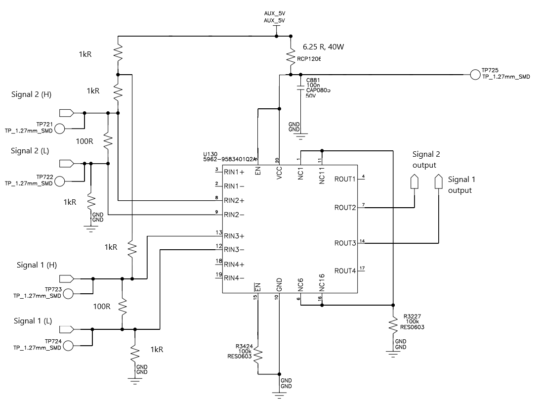
See attached simplified schematic of receiver circuit, if required.
Thanks.
