Part Number: DS90LV001
Hi Experts,
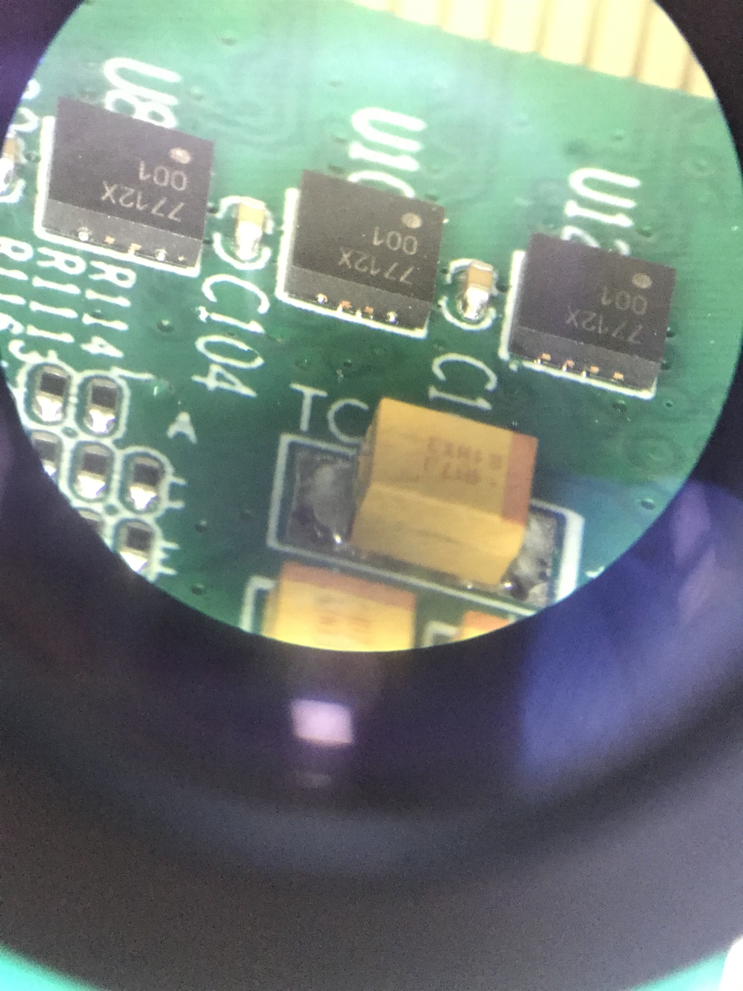
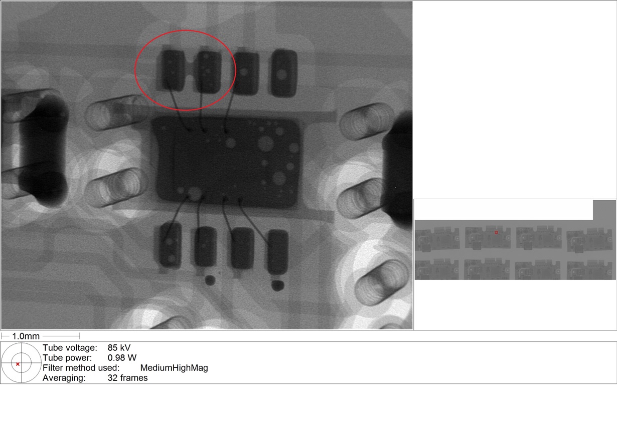
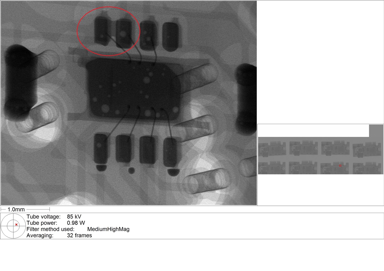
My customer facing pin2 short to ground, they will unsing x-ray to take picture tomorrow. But they want to know why the recommend PCB footprint pad size is equal to chip pad size.
By there knowledge they think the pcb pad should bigger than chip pad , is it right? Do you have suggestion for footprint , or could you give some advice. Thanks


