This thread has been locked.

If you have a related question, please click the "Ask a related question" button in the top right corner. The newly created question will be automatically linked to this question.

DS90UB933-Q1: 933 934 layout review to solve EMI problem

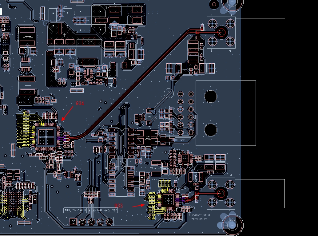
Part Number: DS90UB933-Q1


Hi Team,

My customer met EMI problem when using 933/934 ,which has mentioned in:

https://e2e.ti.com/support/interface/f/138/t/863317

So I ask them for PCB layout to review and  found that It looks OK except the following points:

  • This customer use TOP-GND-POWER-BOTTOM. So as for the high speed signal (Rin/Dout), they lay on the top layer instead of using stripline…

Do I need to suggest them to change stripline? How many layouts do you recommend if using stripline?

  • Buried FPD-Link III High-speed Trace on Signal Layer 1 (the same as the 1st point)

May I ask:

  • Are there other things they need to consider as the  following layout?

Thanks again!

TOP

Layout 2 GND

Layout 3 POWER

BOTTOM

  • Hi Amelie,

    We typically use Microstrip but Stripline should perform fine because the trace is actually buried. I noticed a few things and some other comments that I've mentioned below which might help.

    1) To help narrow down the issue or the location of the issue. We use a flexible EMC Absorber sheet. This can be placed in different regions of the board and you can observed if it changes the frequency that you're failing at. That region will likely be the cause for the issue.

    2) Is the connector backend exposed? and What direction is the field coming from? for example, in the picture you showed, if the field is coming from right to left and hits an exposed connector backend, the noise from that backend could cause issues with your reading. We recommend using a shielded connector to help avoid this.

    3) On the GND layer underneath the high speed, we recommend Anti-Pads or GND cutouts for the PoC network. This will help maintain a 50Ohm impedance when the signal passes by the PoC network.

    4) Are you using a through hole connector? If so, what is the orientation/mounting of the through hole connector? We recommend bringing the signal on the oppoite side of the connector mounting. For example, if the connector is mounted on the top, then the signal should come out from the bottom then got through a via and into the signal pin of the part. This helps avoid creating a large stub where the connector signal pin is placed. A large stub will cause reflections which can lead to noise being radiated during testing.

    5) Please ensure that whether you use stripline or microstrip, 50Ohm impedance is maintained throughout the length of the trace.

    6) We typically use 6-8 layer board, so there's a GND reference for any layers adjacent to the high speed.

    7) To avoid power coupling, I suggest adding a GND reference in between any two power islands that you have on layer 3. I also noticed some yellow traces on the bottom of layer 3, if those are high speed, I recommend having a good ground between that and power. We typically provide a full GND layer just so there's no coupling issues as I mentioned earlier.

    Regards,

    Mandeep Singh

  • Hi Mandeep,

    Thanks for your detail information.

    Wire 1 is  DATA0-7 CLK HS VS.

    Wire 2 is Dout of 934 connected to the connector.

    May I ask:

    wire2 is much more important for EMI comparing to wire1, is it right? Because customer only can keep wire 1 or wire 2 shorter. I recommend they to consider wire2 first and keep wire 2 much shorter first.

    Thanks!

  • Hi Amelie,

    Wire 2 will be more critical in terms of ESD or BCI for the SerDes portion. During ESD for SerDes, you typically try to cause an event on the connector that would be on Wire 2. For testing BCI on just the SerDes, we have to probe on wire 2. In terms of Emissions, Immunity, I say both cases are critical because noise can be contributed from either case (wire 1 or wire 2) and both have to be immune to different frequencies.

    Regards,
    Mandeep Singh