Part Number: HD3SS215
Hi,
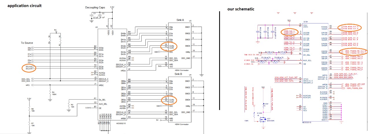
I am using HD3SS215I for one of our applications. I have 1:2 Configuration with HDMI Source and Connectors. One side it is connected to FPGA and other side to connectors. I was facing routing challenges due to criss-cross of data and clock signals. Hence I sapped the connections. DC0 connected to clock and DC1:DC3 connected to data lines. Below is the schematic diagram. I want someone to verify and confirm whether it works.
Regards
Basavaraj