This thread has been locked.

If you have a related question, please click the "Ask a related question" button in the top right corner. The newly created question will be automatically linked to this question.

DS90UB954-Q1: DS90UB953,DS90UB914,DS90UB913

Part Number: DS90UB954-Q1
Other Parts Discussed in Thread: DS90UB934-Q1, DS90UB953-Q1, DS90UB914A-Q1

Hello,team

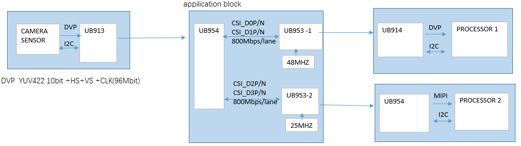
I have some questions about below application block

 1. processor 1 need to configurate camera sensor  through I2C,does this work?how to configurate the serdess ic to support this?

2. CSI_D2P/N and CSI_D3P/N are needed to provide the replicated output of  CSI_CLK1P/N ,does this work?

3. If UB953-1 REFCLK is  48MHZ,Does   UB953-2 need to be the same REFCLK at 48MHZ? Does  the REFCLK of UB953-2  at  25MHZ work?

4..can you give some advices about this application to avoid mistake

best regards

  • Hi, may I know what project are you working? please give me email (steven-shi@ti.com) for detailed discussion. thanks.

    in this thread, please check below comments:

     1. processor 1 need to configurate camera sensor  through I2C,does this work?how to configurate the serdess ic to support this?

    -> yes, it can. this is just same as remote I2C setting issue, you can get the app. note paper on i2c over FPD-Link in www.ti.com. the key settings are:

    in the application block, the UB954 and UB953 should be connected to the same I2C bus.  UB953-1/2 can be the I2C master of the left UB954/its paired ub913a.

    2. CSI_D2P/N and CSI_D3P/N are needed to provide the replicated output of  CSI_CLK1P/N ,does this work?

    -> yes, please check ub954 d/s page6 (When in replicate mode data lanes CSI_D2P/N and CSI_D3P/N are associated with clock lane CSI_CLK1P/N to provide the replicated output. For unused outputs leave as No Connect.)

    3. If UB953-1 REFCLK is  48MHZ,Does   UB953-2 need to be the same REFCLK at 48MHZ? Does  the REFCLK of UB953-2  at  25MHZ work?

    -> ub953-1 and ub953-2 can have different data rate based on external REFCLK.

    4..can you give some advices about this application to avoid mistake

    -> for the link between ub953-1 and ub934, please note the function description in ub953 d/s as shown below, also the app. note SNLA270 is important to guide your design.

    7.4.1.4 DVP Backwards Compatibility Mode
    The DS90UB953-Q1 can be placed into DVP mode to be backwards compatible with the DS90UB934-Q1 or
    DS90UB914A-Q1. While the Mode should have been configured using the Mode pin on the DS90UB953-Q1, the
    register MODE_SEL register 0x03[2:0] can be used to verify or override the current mode. This field always
    indicates the MODE setting of the device. When bit 4 of this register is 0, this field is read-only and shows the
    Mode Setting. Mode is latched from strap value when PDB transitions LOW to HIGH and the value should read
    back 101 (0x5) if the resistive strap is set correctly to DVP External Clock Backwards Compatible Mode.
    Alternatively when bit 4 of this register is set to 1, the MODE field is read/write and can be programmed to 101 to
    assign the correct backwards compatible MODE. This is shown in Table 14.
    CSI-2 input data provided to the DS90UB953-Q1 must be synchronized to the input frequency applied to CLKIN
    when using DVP external clock mode. The PCLK frequency output from the DS90UB934-Q1 or DS90UB914AQ1
    deserializer will also be related to CLKIN when in DVP external clock mode. See Backwards Compatibility
    Modes for Operation With Parallel Output Deserializers (SNLA270) for more information.

    best regards,

    Steven