This thread has been locked.

If you have a related question, please click the "Ask a related question" button in the top right corner. The newly created question will be automatically linked to this question.

PCA9517: PCA9517 --- Please review attached block diagram

Part Number: PCA9517
Other Parts Discussed in Thread: TCA9517

Hi,

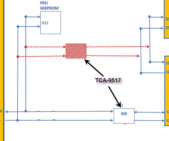
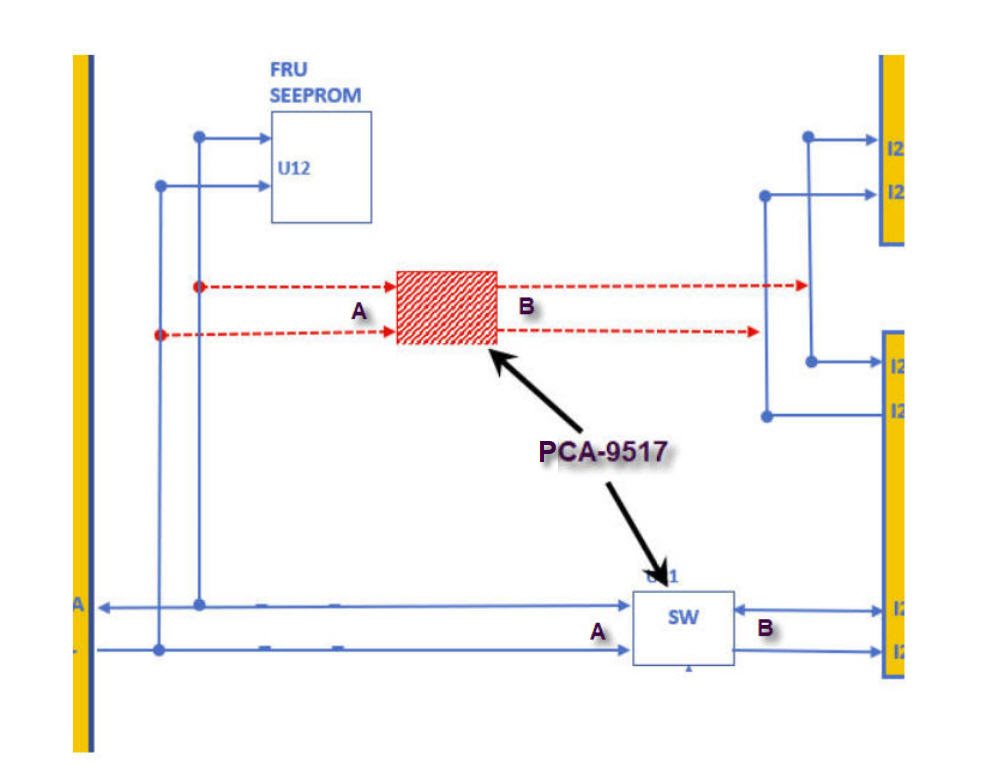
   as I know, there are some limitations on PCA9517 applications. I attached my application block diagram with this message, please review it and tell me whether it is violated any limitations of PCA9517? In our application, we use it as a isolation by enabling/disabling it.

Thanks,

Tony

  • Hey Tony,

    There are some voltage voltage rules on this device which your image does not provide information on the logic levels.

    If you are placing two TCA9517's in contact with each other, the B sides of the devices can NOT connect with each other. Either A to B ot A to A but not B to B.

    B side also has a static voltage offset, so the logic levels on the slave/master on B side should accept ~0.6V as a logic low.

    Also, are you replacing the switch with a TCA9517 or are you placing a switch infront of a TCA9517?

    Thanks,

    -Bobby

  • Hi Bobby,

      Thanks for your quick response.

    On our application, we only connect two A side of PCA9517 together from a I2C master, B side are connected to different I2C slaves.

    The voltage on A side is about +3.0V to +3.3V, B side is about +3.3V.

      Do you see any issues with blow diagram?

    Thanks,

    Tony


  • Hey Tony,

    This should be fine. From the information you provided, I don't see any problems.

    I would suggest our TCA9517 over the PCA9517 as our PCA9517 is NRND.

    Thanks,

    -Bobby