This thread has been locked.

If you have a related question, please click the "Ask a related question" button in the top right corner. The newly created question will be automatically linked to this question.

TCAN1042DEVM: Configuration for the project

Part Number: TCAN1042DEVM

hello,

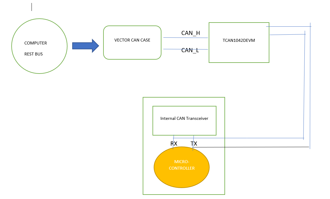
Kindly assist me in configuring the TCAN1042evm for my project.

1. I wish to configure this module with VIo as input for VRXD.

2. Do I need to give a supply to VRXD (3.3V - 5V)

3. with the following configuration, I find the value of VRXD to be decaying, I guess because of the capacitor discharging when I see in multimeter, from 3.3v to 0v.

4. In datasheet it is mentioned, to add C6 capacitor. Can you tell what changes do I have to do if I'm using VIO.

5. Im not using pin 8 of transceiver, I mean STB.

  • Hello,

    To supply a "VIO" reference to pin 5, the best option is to connect pins 1 and 5 of JMP6 to enable the decoupling capacitance and then supply the voltage to the "VRXD" net via either JMP2 or TP8.  Instead of using JMP6, it would also be possible to install a decoupling capacitance at position C6.

    Please let us know if this isn't clear or if you still encounter issues.

    Regards,
    Max

  • hello max,

    1. Why is the RX and TX pin always high(5v)(Recessive), with no CAN signal and only the supply is 5v.

    2. Actually i'm using tcan1042devm to bypass the original transceiver present in my project and using it so as to see the transceiver functioning. I have bypassed rx and tx and am not getting expected output.

    3. Can you please suggest how not to use vio pin of this sensor.

    regards

    ssingh

  • Hello,

    If the TXD is not driven by any other source, it will be biased high by the transceiver.  This results in a recessive level output.  The RXD output will reflect this recessive bus state by remaining high.

    What are you seeing on TXD and RXD that is not expected?  Could you please show a diagram of your connections and any relevant waveform captures (i.e., of TXD, CANH/CANL, and RXD)?

    The VIO pin is a power supply input used for the IO buffers for TXD, RXD, and STB.  The idea is that this voltage could be shared with the IO voltage used by the controller/MCU to ensure logic level compatibility.  The supply voltage should be applied to pin 5 using one of the methods described in my previous post.

    Regards,
    Max

  • HI

    kindly find the block diagram for my project. 

    1. internal can transceiver is TLE8250

    2. THE sensor is power up and so is internal can transceiver.

    3. Internal can transceiver is default 3v3 for VIO pin, and stb pin is also used.

    Provide the configuration of the TCAN1042DEVM that I can use to communicate with my microcontroller.

  • User,

    • Apply 5V to TB1 position labeled VCC, and the GND return path to TB1 position labeled GND, these are both on the silkscreen of the board.
    • Place JMP1 in one of the positions labeled 'PD' on the silkscreen. This will ensure the device is in normal mode.
    • Apply 3.3V to the pin on JMP2 labeled 'P5' and place no shunt on the 4-way jumper JMP6. This will apply 3.3V to the VIO pin (pin 5) if you have the TCAN1042V device.

    The rest is a matter of connecting the correct connections on the micro, which it looks like you have done. Please let me know if you have any other questions.

    Regards,