Part Number: P82B715
1)In the datasheet it is mentioned as "If P82B715 devices are to be permanently connected into a system, the circuit may be configured with only one pullup resistor on the buffered bus"
It means we can provide pull up to lx and ly.
Where sx and sy connected to i2c device without pullup resistor
In this case how the i2c device with open drain input be driven high? can it's working be explained?
Is there any weak pull up internally at sx and sy pins? If yes what is the resistance value
2)As per datasheet "If only a single pullup is used, it must be placed on the buffered bus (as R2 in Figure 5) and the associated total system capacitance calculated by combining the individual bus capacitances into an equivalent capacitive loading on the buffered bus"
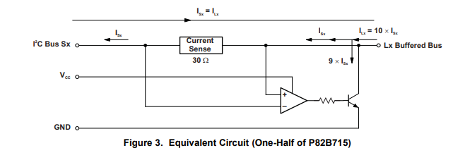
(kindly verify P82B715 datasheet page no 10 for image)
Here why pull up is not provided for clock lines?