Part Number: PCF8574
Hi,
I have two questions about the PCF8574 device:
1.
What are the electrical differences between the PCF8574 and the PCF8574A (beside the address range)?
I'm aware of the document scyb031. In one E2E thread I have read that for new designs it is better to use the PCF8574A. So I assume there are electrical improvements (?).
2.
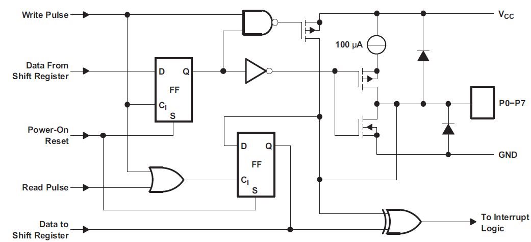
We use 4 of the Port pins as inputs (P0 to P3) and the other 4 as outputs (P4 to P7). On the inputs we have 4 switch connected to GND. After power-up all the port pins act as inputs respective outputs with a weak high-side current source (all the bits have a logic 1).
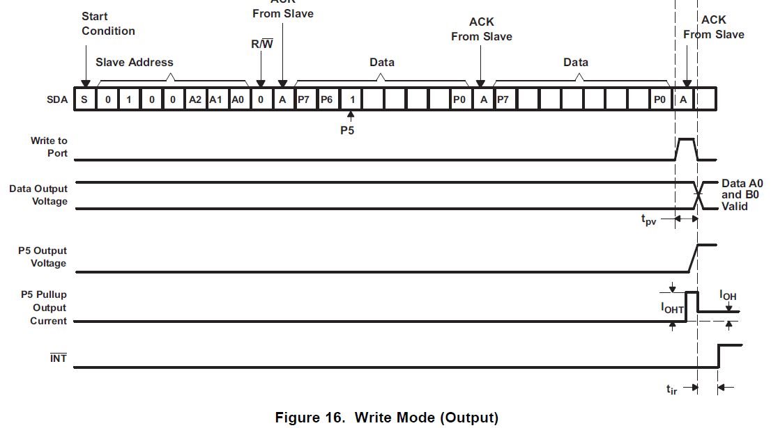
After power-up I need to switch the 4 outputs into a logic 0 state. Therefore I have to write 0x0F to the I/O expander. As of my understandig of the datasheet, while I'm doing that, the lower 4 port pins will activate the second high-side FET for a short period of time (IOHT, in figure 16). Is this current limited to a certain value? All the 4 switch at the P0 to P3 can be closed at this time and therefore the port pins are connected directly to GND. Or does this second high-side FET gets activated only if a port pin has to change from a logic 0 state to a logic 1 state?
Thanks and best regards,
Patrick


