This thread has been locked.

If you have a related question, please click the "Ask a related question" button in the top right corner. The newly created question will be automatically linked to this question.

DS90UB941AS-Q1: query for the operation issue of serdes 941-948

Part Number: DS90UB941AS-Q1
Other Parts Discussed in Thread: CDCEL913

Hi TI,

I have a problem and try to find out the reason. 

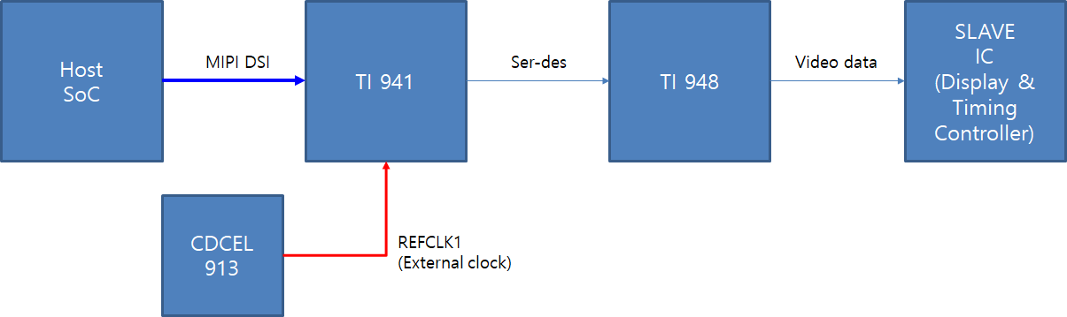
Here is HW system like below. and there are 2x HW board. 

in this same system, same schematic and same HW,

in case of A board, there is no problem, it works well. but,

in case of B board, there is a problem. the problem is "not to show any screen on display panel, in initial time (after booting)". 

our BSP engineer shares : 

- BSP team want to use external clock in TI 941, CDCEL913.

- but, when he(BSP) uses CDCEL913, Board-A shows right image, but, Board-B doesn't show anything in panel during boot sequence. 

- if Board-B uses DSI input clock as the reference clock, display works well. 

- BSP told me that "PCLK_DETECT STATUS" value is different in Board A & B. 
  -> and so, BSP team tries to set the register "PCLK_AUTO (disable), REFCLK (DSI CLK)" in SER 941, and "RX_LOCK_MODE (RX_LOCK asserted when device is linked..)" in DES 948.
  -> in this situation, it works fine. 

My question is : 

q1) is it possible to have different value for "PCLK_DETECT STATUS" in same HW board ? 

q2) is there any point, dependency and pre-condition to use external clock (CECEL913) ? 

Thanks, 

  • Hi Minwoo,

    It sounds from your issue that you might not be following the devices power up procedure properly. Can you check and make sure you are following the datasheets recommended power up sequence in section "10.2 Power-Up and Initialization" . This might be why the two devices are acting differently.

    Regards,

    Michael W.

  • Hi Michael W.

    thanks for your answer.

    I will check Power-up sequence later and then, If I couldn't resolve this issue,

    I will ask it again. 

    Regards, 

  • Hi Michael,

    I have more questions:

    q1) our sw engineer tried and find out some setting for operating, 

    it works well but he doesn't know the reason. 

    He sets below two settings :

    1. [7] bit as 1 on register of BRIDGE_CTL (Address = 4Fh) 

    2. after last setting for ser IC (TX_PORT_SEL Register (Address = 1Eh) ), he gives more delay.   

    how about your opinion ? I guess 2nd setting (more delay) may be effected its power on sequence, you already mentioned. 

    q2) about pixel clock mode :

    in the datasheet, there is a paragraph :

    8.4.2.1 DSI Clock Modes
    8.4.2.2 Pixel Clock Modes
    • 00: DSI Reference Clock Mode
    • 01: External Reference Clock Mode
    • 10: Internal Reference Clock Mode
    • 11: External Reference Clock for Independent 2:2 Mode 

    Exactly I don't know the differentiation on each mode,

    but I think. when I wanna use 'external clock' as pixel clock, can I set the clock mode to "pixel clock mode", instead of "DSI clock mode" ?

    (I can't use DSI clock modes when I use reference clock mode)

    Regards, 

  • Hi,

    When are you enabling the CDCEL913 in relationship to when you are powering on the 941AS? Are you following sequence A or sequence B in section 10.2 of the datasheet? 

    If you want to use an external clock this setting should be set to "External Reference Clock Mode" Can you explain this further? 

    "but I think. when I wanna use 'external clock' as pixel clock, can I set the clock mode to "pixel clock mode", instead of "DSI clock mode" ?

    (I can't use DSI clock modes when I use reference clock mode)"

    Regards,

    Michael W.

  • Thanks for your answer,

    I am checking oh the datasheet and I will ask again for further description.