Part Number: SN75176B
Other Parts Discussed in Thread: SN75175, THVD1550
Hello,
I try to determine the Unit-Load paramter (Input Resistance) of SN75176BP following the description given in
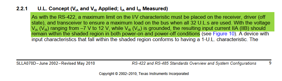
- TIA-485-A-1998, Section 4.1.1 - dc Unit load specification
and article
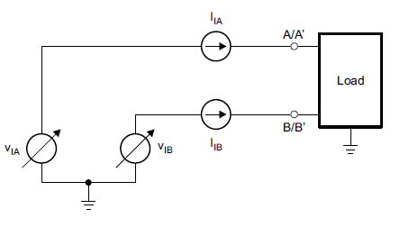
You can determine the unit-load parameter by sweeping the input voltage from -7 to +12V on one bus pin, with the other bus pin held at ground, and then measuring the input leakage current. You will measure both bus pins individually, with the transceiver both in a powered and unpowered state.
and
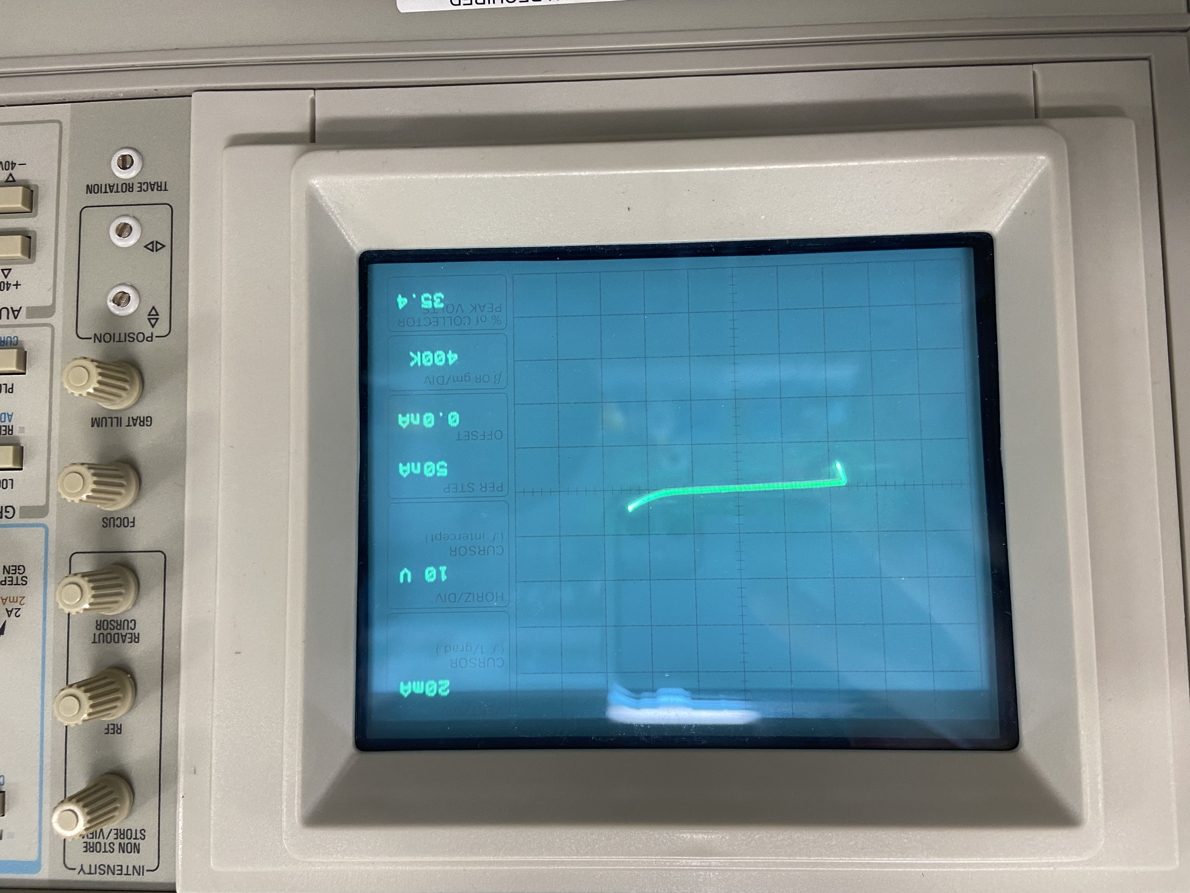
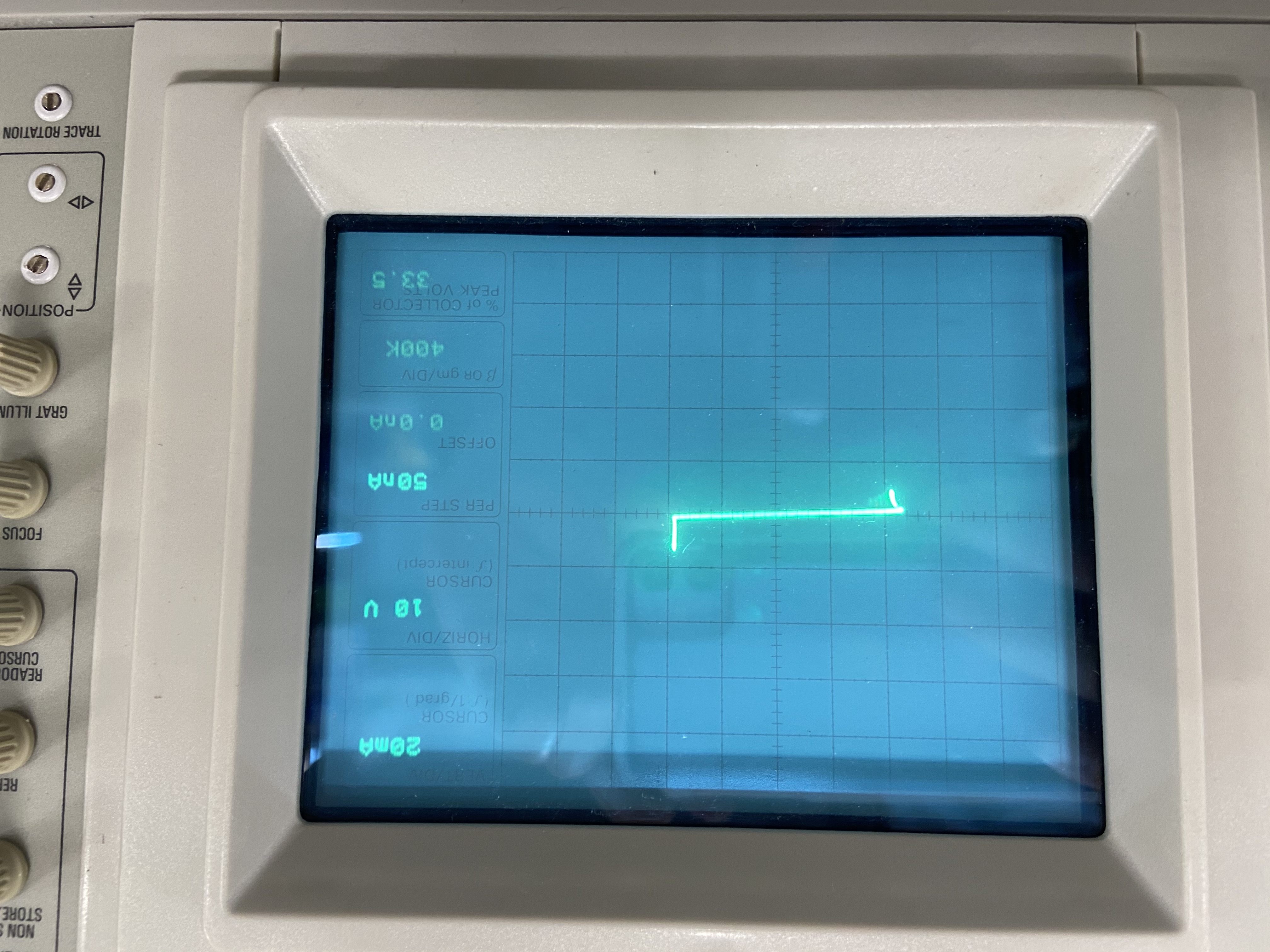
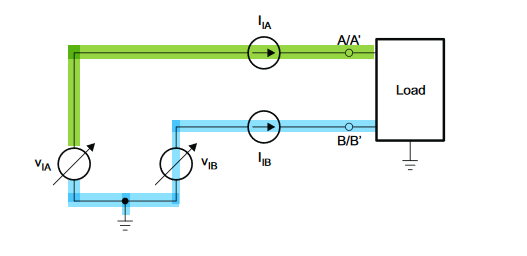
The U.L. Test Circuits I'm refering to are looking like this:
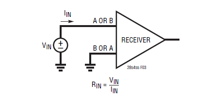
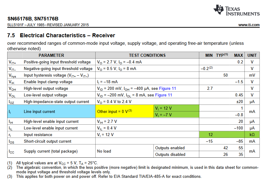
I know that I can get the Line input current / Input resistance from the according datasheet:
and

But as mentioned above I would like to measure the Line input current and calaculate the according Input resistance. For that I created the following two circuits
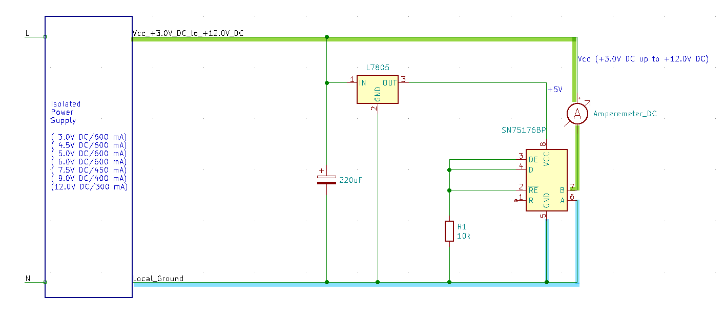
a) Isolated Power Supply / Arduino (Atmega 328p pu microcontroller / SN75176BP
b) Isolated Power Supply / LM7805 / SN15176BP
Vin = Vcc_PowerSupplyOut = 5V / 7V / 9V /12 V
Vcc = Vcc_SN75176BP = 0V or 5V
Driver Enable = low (0V)
Receiver Enable = low (0V)
Data Input = low (0V)
If I'm not mistaken both circuits above should reflect the test circuits mentioned in
- TIA-485-A-1998, Section 4.1.1
- RS-422 and RS-485 Standards Overview and System Configurations, Section 2.2.1 - U.L. Concept (VIA and VIB Applied; IIA and IIB Measured)
- LTC2854/LTC2855, Figure 3. Receiver Input Current and Input Resistance
meaning in order to measure the RECEIVERS Line input current the
- DRIVER needs to be disabled (Driver Enable = low (0V))
- RECEIVER needs to be enabled (Receiver Enable = low (0V))
- Data Input doesnt matter (I put it to low (0V))
My problem is the following:
In case the SN75176BP is unpowered (Vcc_SN75176BP = 0V) everything seems to look ok, I measure as an example 0,85μA having Vin = Vcc_PowerSupplyOut = 11.16 V.
As soon as the SN75176BP is powered (Vcc_SN75176BP = 5V) and applying for example Vin = Vcc_PowerSupplyOut = 9.0 V or 12.0 V the device get's
- extremely hot within seconds
- the Input current measured at A or B is way beyond 300 mA
- eventually the device is damaged and is no longer working
I figured out - or at least it looks to me - that this is happening as soon as I conect either
- Terminal A or B to Ground
- Driver/Enable Inputs to Ground
I'm pretty sure I'm doing something wrong here/the way I think how U.L. test circuits should work but I dont know what. Any help/explanation would be highly appreciated.
Thanks a lot in advance!