Part Number: DP83825I
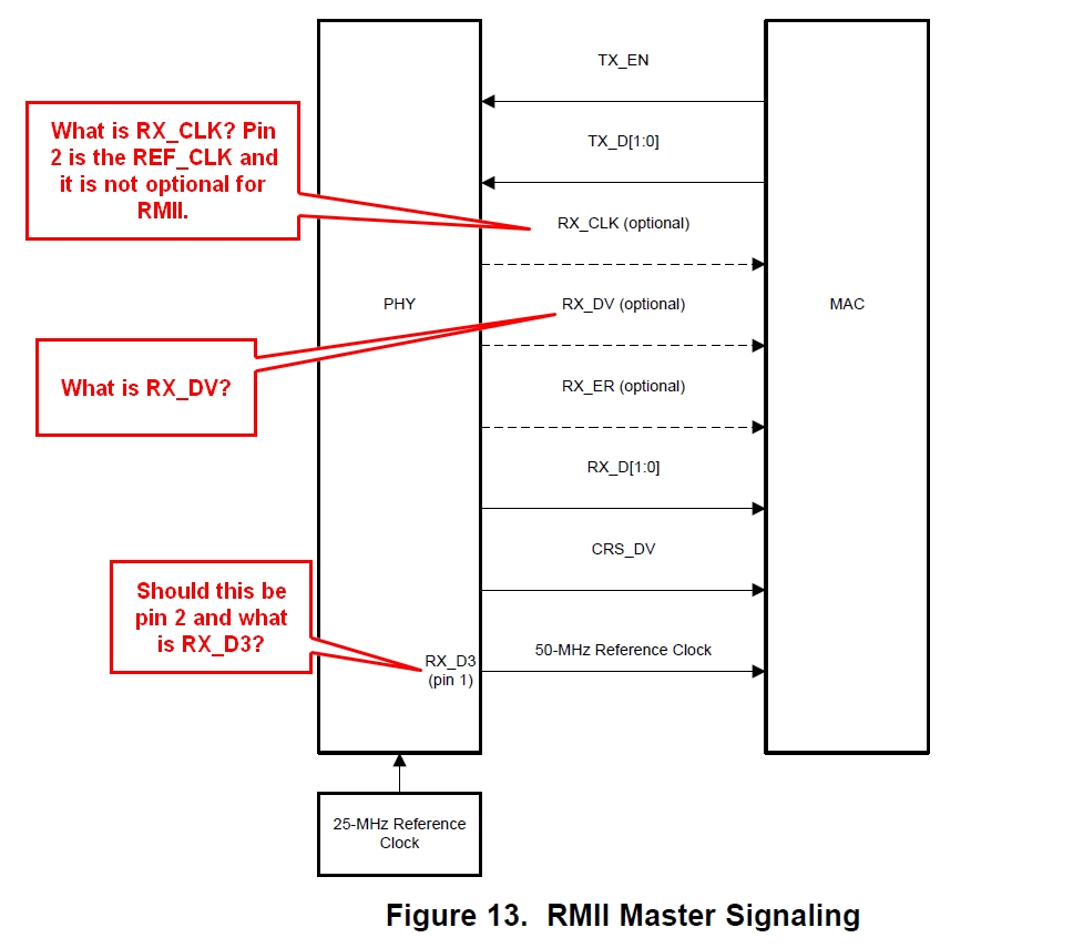
Looking at Fig 13 of the August 2019 version of the DP83825I datasheet, there are several signals that do not seem to make sense. Please see attached picture.
I do not see an RX_CLK signal. The required 50 MHz clock from the Phy is on pin 2. I also do not see an RX_DV signal. The CRS_DV handles this.
I would appreciate any clarification you could provide since we are designing a board for this chip.


