


Part Number: DP83822I
Hi team,
My customer is using DP83822I and using 2 GPIO to mimic a SMI interface to write and read DP83822I. According to below picture in our datasheet, in the read operation <turnaround> stage, MCU will firstly release MDIO to make it in High Z state so it will be pulled up to high state due to the pull up resistor on MDIO. Then DP83822I will respond a bit 0 as acknowledge.

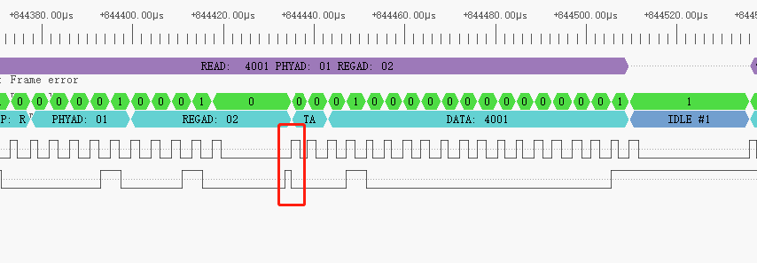
However, in some cases, we use a logical analyzer to capture below waveform. Upper waveform is MDC and lower waveform is MDIO. As you can see from the red circle, DP83822I respond a bit 0 in the first CLK during <turnaround> stage. But in theory, DP83822I should let MDIO stay in high-Z state in the first clk during <turnaround> stage and respond a bit 0 in the second CLK.
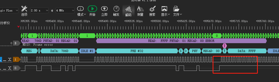
What's more, we also captured another phemonomen as below picture. As you can see, in the <turnaround> stage in red circle, DP83822I didn't respond a bit 0 to acknowledge to MCU which makes the communication failed.
So can you please help check why the above 2 phenomenon happens. Thanks.
Best regards,
Wayne
