This thread has been locked.

If you have a related question, please click the "Ask a related question" button in the top right corner. The newly created question will be automatically linked to this question.

TRS3232E: TRS3232E data DOUT error

Part Number: TRS3232E

Dear team,

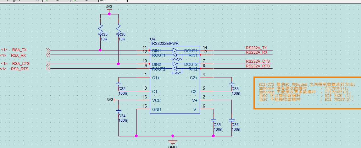
Please review customer schematic as below, customer connect RS232A_CTS  with RS232B_RTS,  they found when RSA_CTS high, but RSA_RTS is low, and RSB_RTS is low.

Customer test CTS independently, they found when RSA_CTS is low, RS232_CTS is not high, but table in datasheet display that RSA_CTS should be high.

Could you give some suggestion? Thanks.

Best regards,

Sammi

  • Hi Sammi,

    We'll get back to you tomorrow with our review of the schematic.

    Regards,

    Eric

  • Hi Sammi,

    The schematic you shared looks good. All pin numbers line up with what is specified on the datasheet, charge pump capacitors are sized and placed correctly, and supply voltage and pull-up values are good. 

    I understand you are experiencing trouble with the device driver and you are not seeing the expected voltage on DOUT2 when DIN2 is toggled. Would it be possible to share scope shots of this driver channel input and output pins so we can see how each pin is behaving? Will you also check the voltages at the charge pump pins (primarily V+ and V-) to ensure that this part of the device is functioning correctly? If these pins are not holding +-5v respectively, please also share scope shots of the other charge pump pins (1, 3, 4, and 5). 

    Regards,
    Eric

  • Hi Eric,

    Thanks for your response. I have not got scope waveform from customer, but they send me the voltage.

    Pin1= 6.0V

    Pin3= 3.27V

    Pin4= 5.95V

    Pin5= -0.13V

    Pin6= -5.63V

    Pin2= 6.07V

    Thanks.

    Best regards,

    Sammi

  • Hi Sammi,

    It appears the storage capacitors on V+ and V- (pin1 and pin6) are generating the correct voltage values. Seeing the scope shots of the input and output pin as well as the other charge pump pins will hopefully reveal more information to help us find a solution. Let me know when this information is available. 

    Regards,
    Eric

  • Hi Eric,

    Thanks for your reply. Customer measure the input and output pin,  when RSB_CTS=3.3V,RS232B_CTS=-5.01V;when RSB_CTS=0V,RS232B_CTS=-5.01V; seems that input changed but output has not changed. I am not sure if this helps.

    Thanks.

    Best regards,

    Sammi

  • Hi Sammi,

    Since you are seeing a ~-5 V output we know the chip is properly powered and the charge pump is working.  For some reason it is just behaving as though the DIN port of interest is at a high level even when 0 V is measured.  Are you seeing this consistently across multiple PCBs/units?  Is it possible that this is simply a connection issue (e.g., bad solder joint)?

    Regards,
    Max