This thread has been locked.

If you have a related question, please click the "Ask a related question" button in the top right corner. The newly created question will be automatically linked to this question.

TPD4E05U06: Impedance issue

Part Number: TPD4E05U06
Other Parts Discussed in Thread: TPD1E05U06

Hi, 

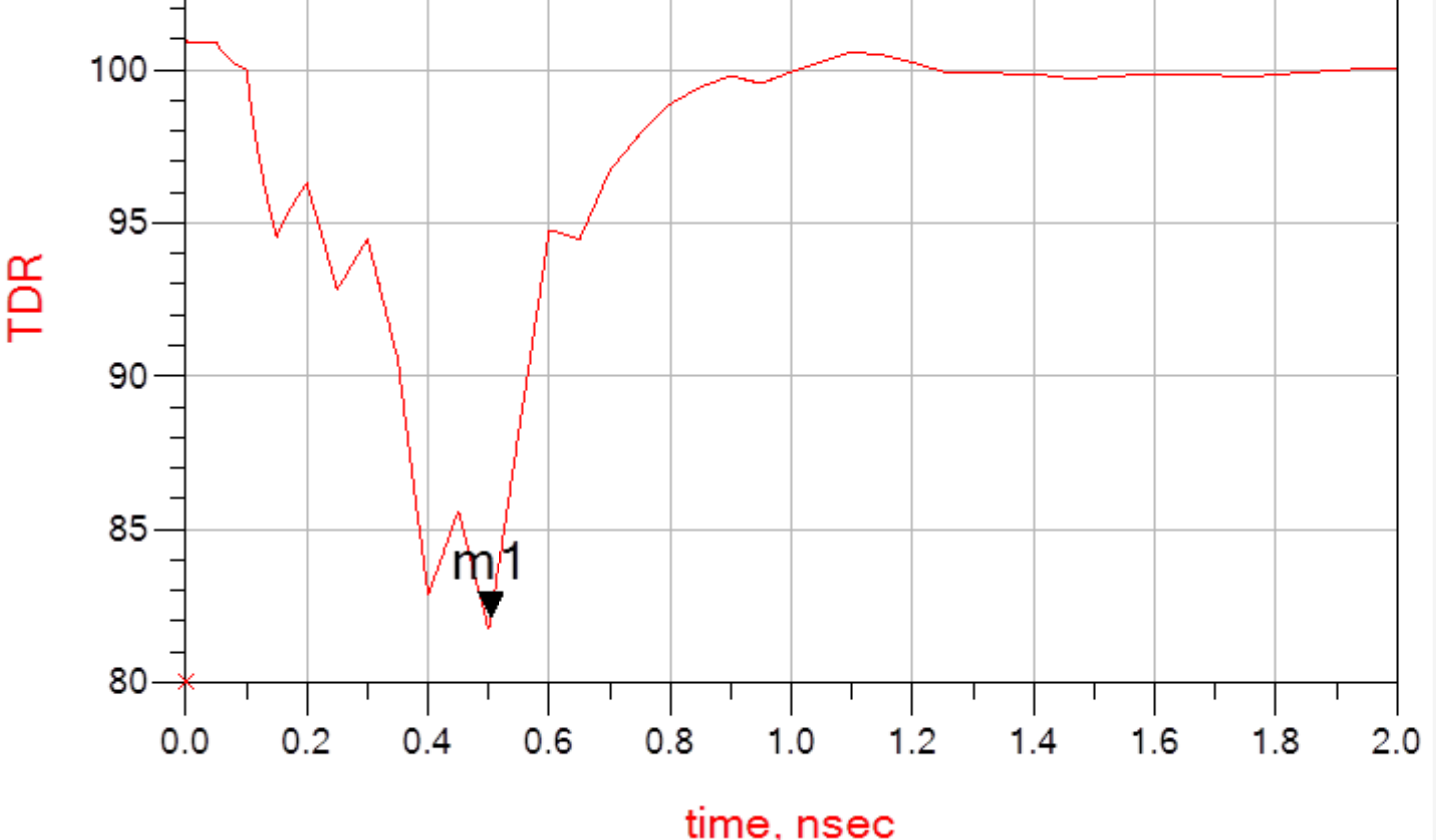
Can you confirm the s-parameter port mapping for the TPD4E05U06? The file has two ports - do these correspond to Dx and NC or Dx+ and Dx-. Can you also specify which is the input and output.

I'm getting some odd impedances when simulating with this device - could someone get in touch to discuss offline? 

Many thanks

  • Hi,

    Attached will be the appropriate file for the s parameter of the TDP4E05U06.

    Port 1 is input1; Port 3 is output 1

    Port2 is input 2; Port 4 is output 2

    Let me know if you have any questions!

    Best regards,

    Andy Robles

    TPD4E05U06.zip

  • Hi Andy, 

    Thanks for your response on this. 

    I notice your zip file contains a 4 port model - could you elaborate how the input and output ports relate to the real life schematic? Is the input the Dx+/- pins and the output the corresponding NC pins? 

    Should I be using the model you provided over the 2-port version on the product page? Is the number of ports (and their interactions) the only difference?

    Many thanks

  • Hi,

    The 2 port file provided in the product page corresponds to the TPD1E05U06 which only has one channel of protection. The file I provided will serve as the functionality of the TPD4E05U06 for D+ and D- signals.

    The inputs will be the D+ and D- signals before they pass through the TPD4E05U06 and the outputs will be the signals after they have passed through the device to show how the device will be affecting them. The outputs do not correspond to the NC pins.

    Let me know if you have any questions.

    Best regards,

    Andy Robles

  • Hi Andy, 

    Thanks for the clarification on the above. Running a TDR test on these s-parameters, I find that using 1/2 as inputs and 3/4 as outputs, I see a positive deviation in the impedance. This is simulating an ideal transmission line with just these s-parameters and a 100R terminator.

    The impedance is around 120ohms for a 200pS rise time which seems a little unusual as with other similar diodes in this range, I've been finding that they actually introduce a large dip in impedance which I'm assuming is down to the additional capacitance they add to the channel. 

    One thing I noted was that the attached model is not reciprocal and so re-simulating with ports 3/4 as the inputs and 1/2 as the outputs causes an impedance dip similar to what I've seen with other devices. Could you double check the port assignments are definitely correct and that they've not somehow got mirrored?

    Many thanks

  • Hi,

    When viewing the S-paramter using 1/2 as inputs and 3/4 as outputs or vice versa will not affect the data shown. This should also mirror to the TDR test, but after doing the simulation I noticed that is not the case. Please use the configuration with ports 3/4 as the inputs and 1/2 as the outputs to acquire the correct TRD analysis data. Here is what I obtained after doing a quick simulation. Do you get similar results in your test?

    Best regards,

    Andy Robles

  • Hi Andy,

    Thanks very much for confirming the above. Yes I get a similar(ish) shape to what you have above. The impedances I see are slightly different - could you confirm the rise time you are using for this simulation? 

    Finally, I'm still a little confused as to how these s-parameters should be connect in my extracted transmission lines. As these TVS diodes are typically used by connecting between the signal and GND, am I right in thinking that I should connect this s-parameter model in parallel with the diode pads. For example, port 3 should connect to TPD4E05U06 Dx+ land pattern pad and port 1 to TPD4E05U06 NC land pattern pad? 

    Many thanks for your help.

  • Hi,

    For this simulation I used a 200ps rise time which could explain the differences in the results.

    The NC pins in our ESD devices are not connected to the internal circuitry of the device. The input and output come out of the same pin of the TPD4E05U06. The input will be the data signal before it passes through the TPD4E05U06, and the output represents the signal after the insertion loss of the device due to its capacitance.

    Best regards,

    Andy Robles