


I have an old keyboard, an IBM Model M produced by Lexmark to be exact, that I am trying to convert from PS/2 to USB. Instructions for doing this by using an active PS/2 to USB converter are available elsewhere but not for this specific model which uses a different PS/2 chip than the others shown in the instructions. What I need is either some help in identifying the PS/2 clock and data pins or a datasheet, for the PS/2 interface chip on the PCB.
I have already looked around on the Internet and TI's site but have found no clues so far. Here is a pic of the IC.
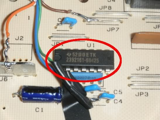
The markings on the IC are: 52D0ETK (or 52DOETK) and 2392161-60425
One of the PS/2 wires goes into the IC at pin 2 and 3 while the other is connected at pins 5 and 12. Both have a capacitor going to ground and a resistor (the blue package) going to VCC(+5 VDC) connected in parallel.
Pin 7 is connected to GND and pin 14 is connected to VCC.
Besides the VCC, GND, PS/2 Clock, and PS/2 Data, it also has 8 pins which all seem to connect to the primary controller chip for the keyboard which most likely are D0-D7 or D0-D6 with a selector or modifier bit connection.
Sorry if this might be in the wrong forum. Please move it if it is.
