This thread has been locked.

If you have a related question, please click the "Ask a related question" button in the top right corner. The newly created question will be automatically linked to this question.

TCAN1043-Q1: About TCAN1043 Block Diagram

Part Number: TCAN1043-Q1
Other Parts Discussed in Thread: TCAN1043

Hi all,

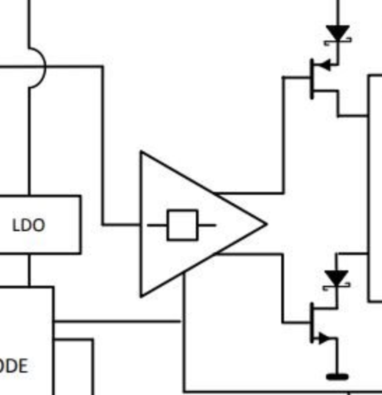
This is TCAN1043 Block Diagram.

I had some questions, while I looked the datasheet.

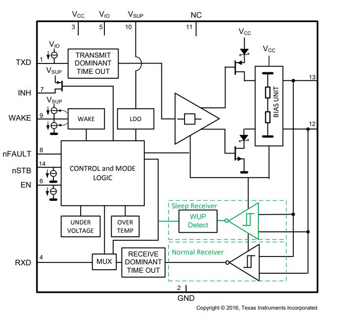
Could you please explain what and how the "Biass Unit" Box works?

What is the "WUP Detect"?

Can you explain me how the MUX works in this block diagram?

Thank you.

  • Gary,

    The bias unit is the circuit that biases the CAN bus to the ~2.5V recessive level when the transceiver is not driving the dominant bus level.

    WUP detect is the detection circuit for the specific wake-up signal on the CAN bus. This signal is defined in the ISO11898 CAN specification, and consists of a dominant-to-recessive-to-dominant pulse on the bus what the transceiver is in standby for sleep mode.

    Are you referring to the WUP detect vs. normal receiver? The normal receiver is disabled in low-power modes (standby and sleep), so all CAN signals then go to the WUP detect block. During normal and silent mode, all CAN bus messages go through the normal receiver.

    Please let me know if you have any other questions.

    Regards,

  • Thank you for the response, Eric.

    What is the 2 of square boxes in the Bias Input block, are those resistors? how the "Bias Input" block biases can bus to 2.5v?

    Is this comparator on the left of FETs on below picture? Could you please explain how the comparator works from the TXD signal?

  • Gary,

    The two square boxes in the bias unit are meant to represent a resistor divider created to split the 5V VCC to create VCC/2 that the CAN bus pins are biased to when they aren't driven dominant.

    The comparator is what drives the FETs when the TXD signal meets the logic threshold for a dominant bit on the bus. So when the voltage level on TXD is 0.7*VIO or higher, the comparator will interpret this as a recessive level and the FETs will not be driven. If the voltage level on TXD is 0.3*VIO or lower, the comparator will interpret this as a dominant level and the FETs will be driven to drive a dominant signal on the bus.

    Regards,

  • Thank you Eric,

    so if TXD is high voltage signal, 5v Vcc(upside of "bias unit" box)  goes to the resistor divider, and makes recessive signal which is the 2.5v(Vcc/2), correct?

    if TXD is lower voltage signal, (Vcc(upside of FET) + Vcc(upside of "bias unit" box))/2 = Vcc(5V) goes to the CANH, and how the CANL 0v can be made?

    Thank you

  • Gary,

    You are correct, the recessive level is indeed 2.5V.

    For the dominant signal, both FETs are driven so you'll have CANH being pulled up to VCC and CANL pulled down to ground, completing the circuit and allowing current to flow through the load (termination) resistance on the bus. If we assume the load resistance is 60Ω, and the RDSon of both FETs is 20Ω, then that gives a total of 100Ω. With about 0.5V drop from each diode, that gives a full 1V dropped from the 5V of VCC. So you have 4V/100Ω = 40mA. With the 40mA through the 60Ω resistor, a 2.4V drop occurs over the termination resistance, driving CANH to 3.5-3.7V, and CANL to 1.3-1.5V. 

    Because of the diode voltage drops and the voltage drops over the RDSon internal to the CAN transceiver, CANH won't pull up to the full 5V of VCC, and CANL won't pull down completely to GND. The example I used assumed quite a bit for the values for easier calculations, and was assuming a nominal case.

    Please let me know if you have any other questions.

    Regards,