This thread has been locked.

If you have a related question, please click the "Ask a related question" button in the top right corner. The newly created question will be automatically linked to this question.

TCA9800: Vol of TCA9800

Part Number: TCA9800
Other Parts Discussed in Thread: TCA9803

Hi team,

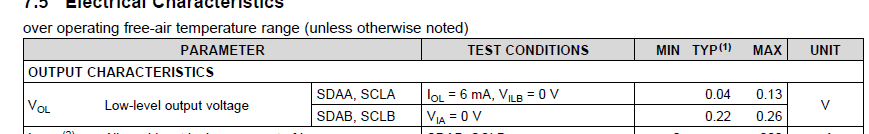
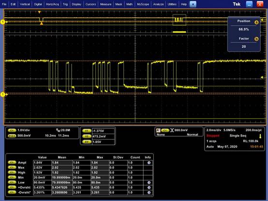
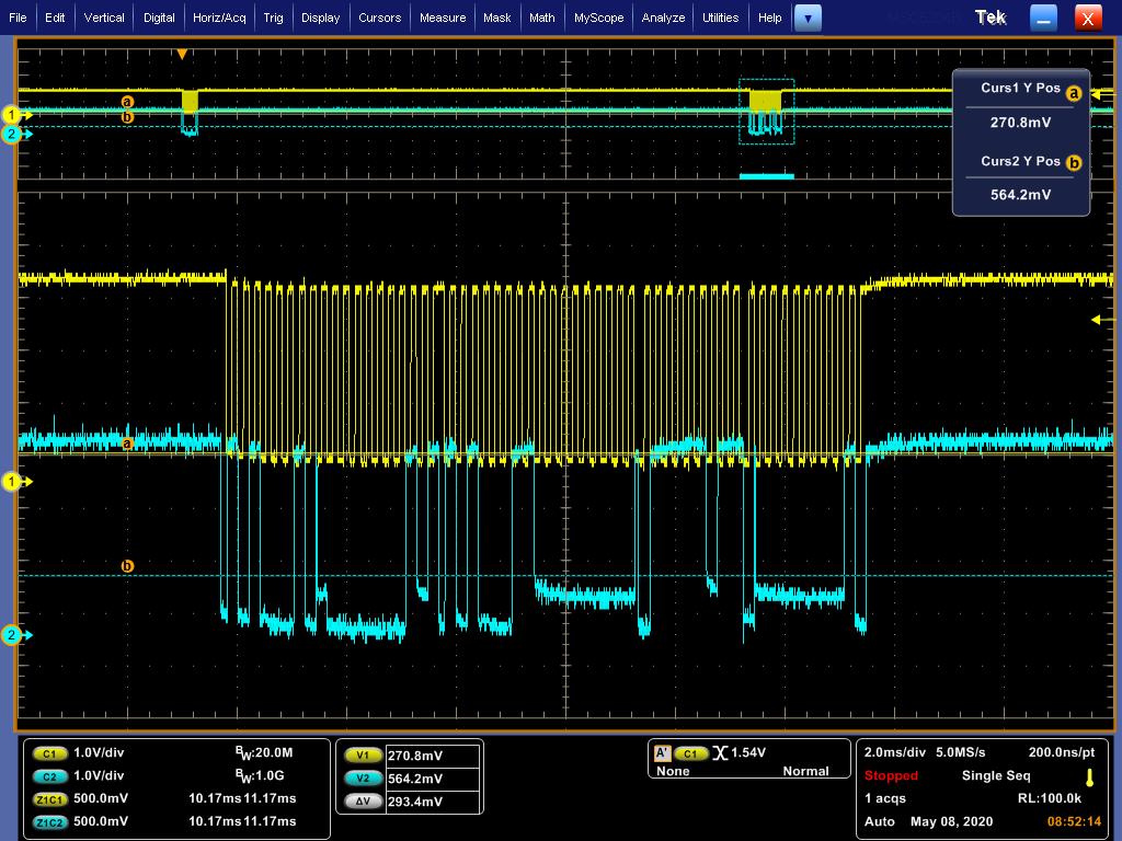
My customer is using the TCA9800 now. The B side has no series and pull up resistors. But the Vol still has some stages which is about 400mv. Based on the datasheet, the Vol should be less than 220mv. Do you have some ideas about the phenomenon? Thanks.

  • Frank,

    Can you provide a block diagram of the I2C bus?

    My initial guess is you have a device on the I2C bus that has a very large VoL (weak pull down) or master/slave with a series resistor infront of its SDA pin.

    Please also include a scope shot with both SDA and SCL in one picture. To me, I can see the driver is switching and you a re just saying two different VoLs from another source.

    -Bobby

  • Hi Bobby,

    I have mentioned in the first post, no pull up and pull down resistor and no series resistor. i will share the scope shot later. Thanks.

  • Based on the bit analysis, the shifted levels are coming from a separate driver (that is the slave is generating the higher VoL).You can tell because after every 8th clock pulse (the ACK) the ~440mV signal is generated when our device releases the bus. You can also see that after the read (green 'R') the signal stays at ~440mV meaning the slave is now driving the signal because the slave takes control of the data line.

    From the block diagram you state 1.8V logic on B side and 3.3V logic on A side, the scopeshot shows 1V/div which means the scope image is of A side. So a slave on A side is generating the ~400mV signal, not our device. If you change the pull up resistor on A side, you can make the VoL lower. 

    -Bobby

  • Hi Bobby,

    Thanks for your reply. It's my mistake not describe very clear. The voltage is 0.5V/div(ZICI,Z2C2),not 1V/div. And FPGA is the master, our device is the slave. So the ACK should be generated by TCA9800 not FPGA. So the Vol of TCA9800 is about 400mv. Thanks.

  • Hi Bobby,

    Do we have some update? Thanks.

  • Hey Frank,

    Is it possible that the FPGA has an internal pull up resistor enabled? If so, this would shift the VoL of our TCA9800 up due to the additional current being sourced externally.

    Is it possible for you to remove the FPGA and then pull the A side to GND and measure the VoL on B side to confirm if the VoL is still ~400mV? Or you could remove our device from the main board and place it on a break out board and hold A side to GND then measure B side VoL. If you see the voltage go down to ~200mV doing this test/check then it is likely there is an external current source on B side somewhere shifting our VoL up.

    Another potential option is to change the TCA9800 to TCA9803 and see if the VoL gets lower on B side on the main board. This should occur because the drive strength on B side is stronger and an external current source would have less effect on the VoL on B side.

    -Bobby

  • hi Bobby,

    i have applied the TCA9803 sample for the customer to do the tests. Thanks.