This thread has been locked.

If you have a related question, please click the "Ask a related question" button in the top right corner. The newly created question will be automatically linked to this question.

SN75DPHY440SS: CSR register no convetion detected

Part Number: SN75DPHY440SS

Hi,

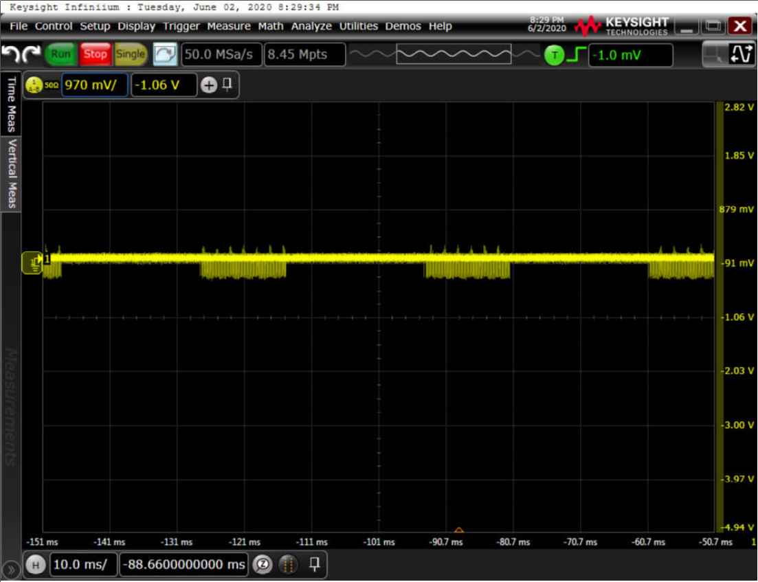
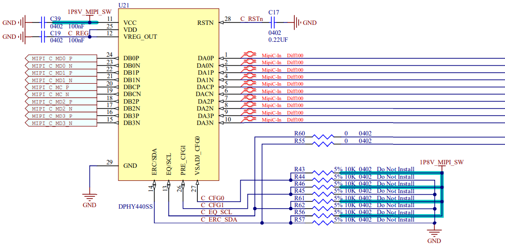
I am trying to use SN75DPHY440SS MIPI retimer with 250Mhz MIPI clock and 1-4 MIPI Data lane cameras. There is not output from the retimers, and CSR register "0D" returns x"20" which per datasheet means ,,no convetion detected". I checked input to the retimer and everything seems fine, retimer is connected as recommended in datasheet. 

Thanks.

  • Hi,

    Register 0x0D returns a value of "0x20", means there is contention detected on the DB0N. Because the 0 lane supports bidirectional LP communication, it means someone else is driving the 0 lane. Can you use a scope to probe the 0 lane?

    Thanks

    David

  • Hi David,

    bellow is the image from the osciloskope with the differential probe.  

    Is there a way to disable bidirectional LP communication ? Also, how is direction of communication detected on chip ?

    Thanks. 

  • Hi,

    With Lane 0 path (DA0P/N and DB0P/N) supporting bi-directional LP signaling, it is very important that DB0P/N LP TX is connected to an unterminated LP RX. 

    You can use the following I2C register commands to enable lane0 HS path:

    Enable HS path for Lane 0 only:

    Write Register 0x50 with 8’h01 //Override enable for HS TX path

    Write Register 0x51 with 8’h01 //HS TX path enabled.

    Write Register 0x61 with 8’h00  // Disable LP path.

    Write Register 0x70 with 8’h01  //Override enable for HS RX path

    Write Register 0x71 with 8’h01  // HS RX path enabled.


    Bit 0 is lane 0

    Thanks

    David

  • Hi David,

    this unfortunately did not solve our problems. 

    Since we are using cameras we want DA0 LP to always be in RX mode and DB0 to be in TX mode and disable contention detection.

    This is how we connected retimer. 

    And this is how we connected retimer outputs to the FPGA, note that each of the lines is connected to inputs 2 pins, one being LP(K18, J18) and one being HS(H18, G18). Without timer this approach of two pairs of input pints works fine for us. Is it possible it is creating contention even tough both pairs are inputs?

    Thanks.

  • Hi,

    The DB0P/N LP TX must be connected to an un-terminated LP RX.  If DB0P/N LP TX is connected to a HS RX, then LP signaling will not be able to reach the LP11 levels and which will cause the DPHY440 to not enable HS data path on Lane0. How are you handling the LP and HS RX in the FPGA for lane 0?

    Thanks
    David

  • Hi David, 

    As Vuk mentioned we are using two sets of input pints where one is declared as LVDS input (per EIA-644 standard), and the other one as SSTL-2 Class I input (per JESD8-9B standard). We have been using this approach and it worked just fine with different kinds of imaging sensors. However this is our first application with DPHY440 retimer and seams like there are issues.

    We are observing D0 never goes to HS mode, but stays in LP00. 

    As we are having CSI-2 application that doesn't need bidirectional LP. is there an option to disable contention detection and force A->B direction. Could you please tell more about registers x50, x51, x60, x70, x71 - we have hard time following comments. 

    Any other ideas are welcome. If possible, we would like to schedule a call to discuss issue furthermore. 

    Looking forward to hear back from you!
    Marko 

  • Marko

    The command I provided earlier would disable the DPHY440 LP TX on DB0P/N and only enable the HS TX and RX. Are you disabling the LP RX and only enable HS RX in the FPGA?

    Thanks

    David

  • Hi David, 

    No, we are having them both LP RX and HS RX always on.

    Thanks

    Marko

  • Hi David, 

    Could you please additionally explain definition and application of LP Logic 1/0 contention thresholds?

    Is there a document describing undocumented i2c registers that we could have for assistance? We can sign NDA if required. 

    Is there a way to disable D0AP/N LP TX and D0BP/N LP RX ? 

  • Marko

    When the DPHY440 powers up, its LP TX is expected to see an un-terminated LP RX or high impedance, If it's not seeing the high impedance, then it will assume someone is driving the bus and set the contention bit. 

    Write Register 0x61 with 8’h00 will disable LP B0 TX

    Write Register 0x7E with 8'h00 will disable LP A0 RX.

    I attached a Xilinx FPGA MIPI implementation for your reference: https://www.xilinx.com/support/documentation/application_notes/xapp894-d-phy-solutions.pdf.

    Thanks

    David 

  • Hi David, 

    Thank you for reply. 

    Please note we would like to try the opposite - disable LP A0 TX and LP B0 RX - is this an option?

    Also, Is there an option to clear contention bit trough I2C commands (after sensor stream has been turned off) ? at the moment we have to reset chip to clean up the error..

    Thanks
    Marko 

  • Marko

    I made a mistake in my previous response.

    You only need to 

    Write Register 0x61 with 8’h00 to disable the LP path for all channels.

    Once the LP is disabled, then you will not see the contention error.

    Thanks

    David

  • Hi David, 

    We are seeing contention error even with LP disabled. Also, our receiver cannot decode MIPI without LP. We are looking at mid-point solution where we are just disabling LP B0 TX by writing register 0x61 with 8'h1E. However we dont have working solution yet. Meticom chip app note suggesting is something we have considered in the past and dropped it. 

    We would be happy with if we could disable LP A0 TX and LP B0 RX - is this an option?

    Regards,
    Marko

  • Marko

    There is no option to disable the LP A0 TX and LP B0 RX. In the FPGA, can you disable LP and enable HS only?

    Thanks
    David