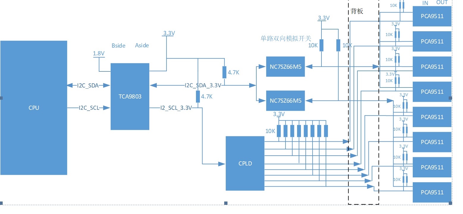
The figures below present a partial view of the schematics I am working on:
My questions:
Is the connection between TCA9803 and PCA9511 OK?
Thank you in advance for your support.
This thread has been locked.
If you have a related question, please click the "Ask a related question" button in the top right corner. The newly created question will be automatically linked to this question.
The figures below present a partial view of the schematics I am working on:
My questions:
Is the connection between TCA9803 and PCA9511 OK?
Thank you in advance for your support.
Hi Seasat Liu,
Can you please explain quite a bit elaborate? I have few question regarding the usage of NC7SZ66M5 and CPLD. How the NC7SZ66M5 switch is handled with I2C data alone? If it is like complele I2C switch both data and clock need to be handled Am I right? SDA total pull up will be 5kOhm since two 10kOhm added in parallel. So please check that is fine for you. Please let us know the CPLD and NC7SZ66M5 usage !!
Thanks,
Vignesh.M
hi Vignesh.M
This is my description. If you have any questions, please contact me
1. Since the data line is double-wired and the clock line is unidirectional, it is handled separately.
2. There are 8 daughter cards on the I2C bus, and each daughter card passes through the PCA9511 chip first.
3. The data line is controlled by the analog switch NC7SZ66M5. Because of the wiring across the backplane, two analog switches are used. Each NC7SZ66M5 controls 4 slots of sub-cards. The default state is off (high impedance). When the CPU needs to access, choose to open one of the switches.
4. The clock line goes through the CPLD logic to complete the 1 FANout 8 function. The SCL output by default is also off (high impedance), and the corresponding channel SCL will be opened only when the CPU needs to access which way.
5. During CPU access control, the SCL and SDA strobes are controlled at the same time, and the layout length and logic internal delay of SCL and SDA are not deliberately controlled.
Hi Seasat Liu,
Thanks for your clear explanation..!!!
I2C clock will be bidirectional in the below functionality,
1. Clock stretching 2. Multi master mode.
I think it is good to considering the clock as bi-directional signal instead of unidirectional.
And why can't you try to use single 8 channel switch PCA9548A ?
Let me know your thoughts.
Thanks,
Vignesh.M
Seasat Liu said:Part Number: TCA9803
The figures below present a partial view of the schematics I am working on:
My questions:
Is the connection between TCA9803 and PCA9511 OK?
[Bobby] A side of TCA980x to a pass FET into a PCA9511 is okay.
I only have 2 additional comments here:
(1) Why use the NZ7SZ66? I would think something like PCA9306 would be better as it gets rid of an additional discrete component.
(2) TI has a pin to pin replacement for the PCA9511 which we call the TCA9511A which has wider Vcc range, higher temperature support, and better dynamic offset voltage than the PCA9511. Between the two, it would make more sense to use the TCA9511A.
Thank you in advance for your support.
-Bobby
HI Bobby
1) Why use the NZ7SZ66? I would think something like PCA9306 would be better as it gets rid of an additional discrete component.
If we do not use this switching device, there are 8pics PCA9511 loads across the backplane of the SDA line, and the signal quality may not meet the standard; after using the switching device, there are only 4pics loads on the SDA; if we use PCA9306, it should not solve the SDA driving capability. problem.
(2) TI has a pin to pin replacement for the PCA9511 which we call the TCA9511A which has wider Vcc range, higher temperature support, and better dynamic offset voltage than the PCA9511. Between the two, it would make more sense to use the TCA9511A.
In the CTM system, PCA9511 and TCA9511A are the same AVL code and are not distinguished. According to the price, the market share is decided by CTM sourcing