


Part Number: DP83826I
Hello Team,
I have inquiries about DP83826I.
(1) DP83826 & DP83822 have similar specifications. What is the background of DP83826I development ?
(2) About the power supply sequence.
In customer's application, the clock is not input to XI during 3.3V power rising.
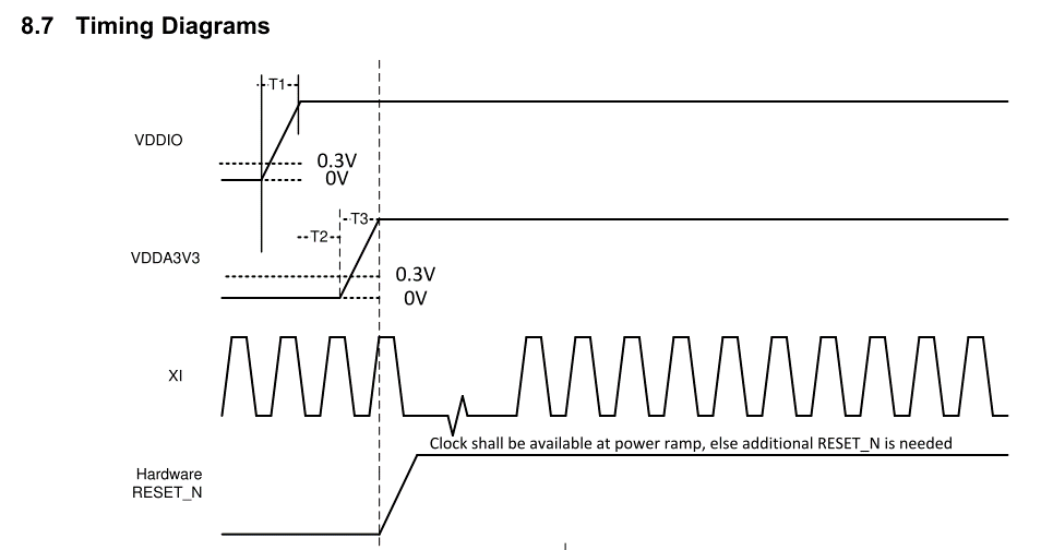
I belive the following sequence is required to keep the instruction "Clock shall be available at power ramp, else additional RESET_N is needed".
1. 3.3V power supply (VDDIO, VDDA3V3) turns on. At this time, XI pin is fixed at 0C.
2. Clock input to XI.
3. Reset release (Hardware RESET_N rise)
Is this sequence correct ?
(3) If fast link drop is enabled in the bootstrap of RX_D3, are the following three Fast Link down modes enabled?
• RX error count
• Low SNR threshold
• Descrambler link loss
(4 If RX_ER During IDLE = Disable (0x0A bit2 is 0), Will the link be down due to the RX error count condition even during the IDLE period?
When RX_ER During IDLE = Disable (0x0A bit2 is 0), I concern that RX_ER will not be detected during IDLE, and then link down will not occur under the condition of RX error count.
Any advice will be appreciated.
Jin

