Part Number: TCAN4550
Hi,
We are using TCAN4550 with ST MCU.
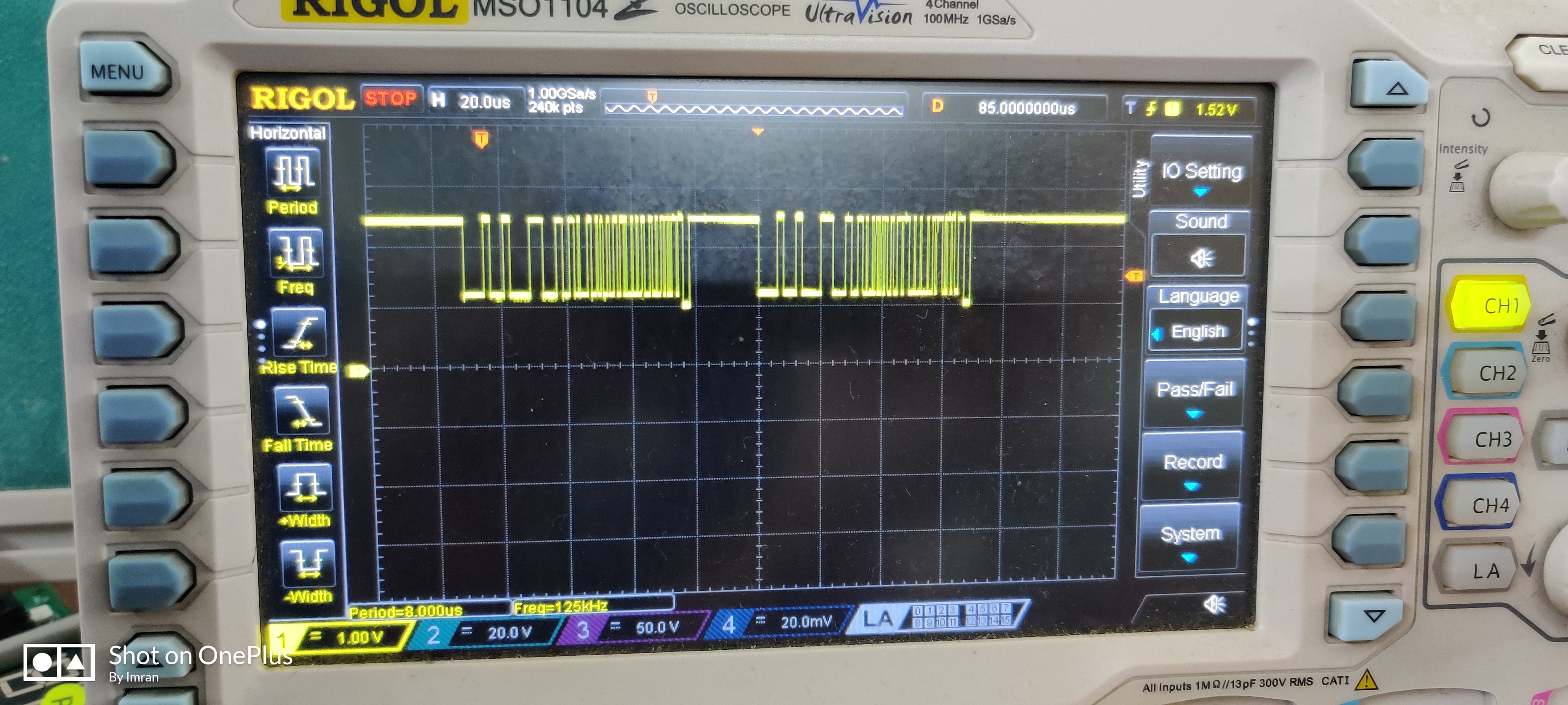
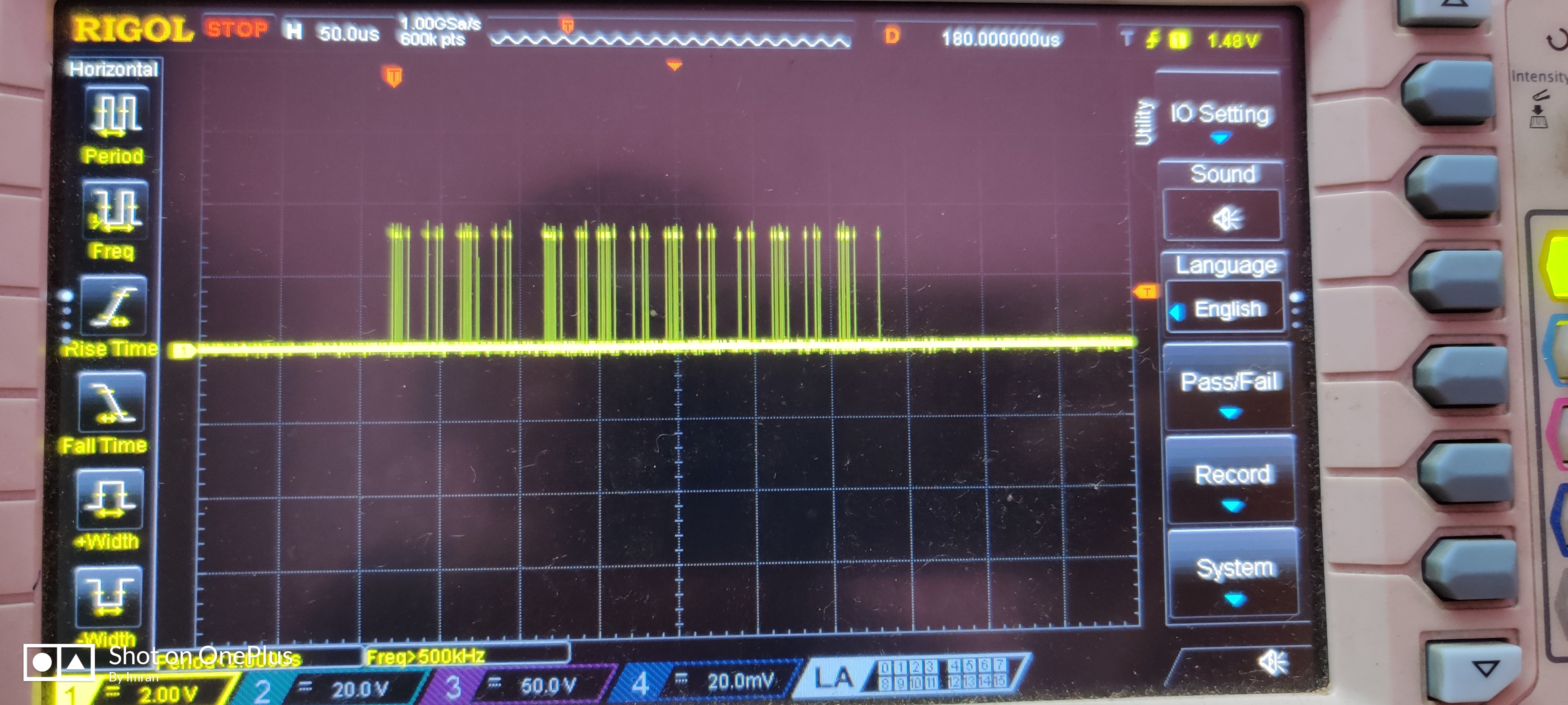
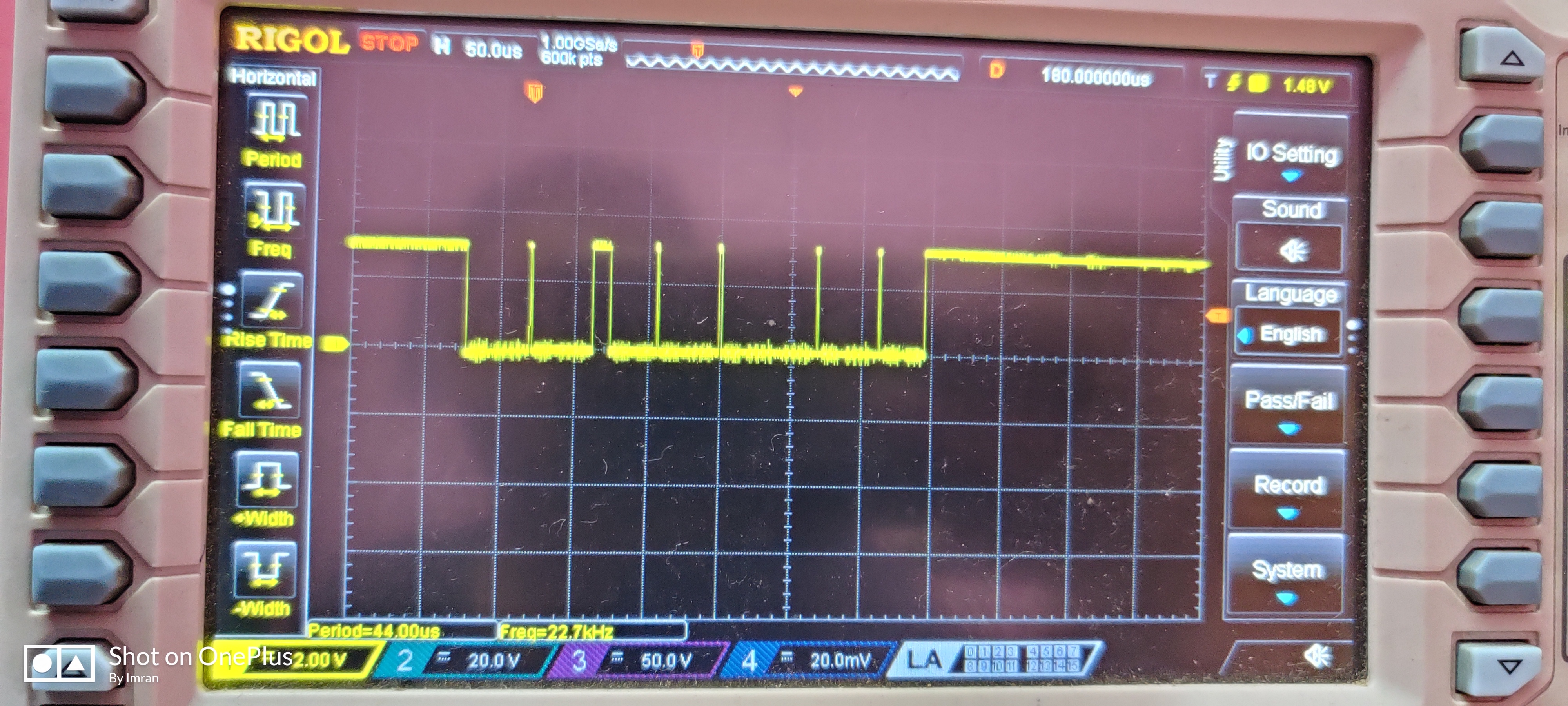
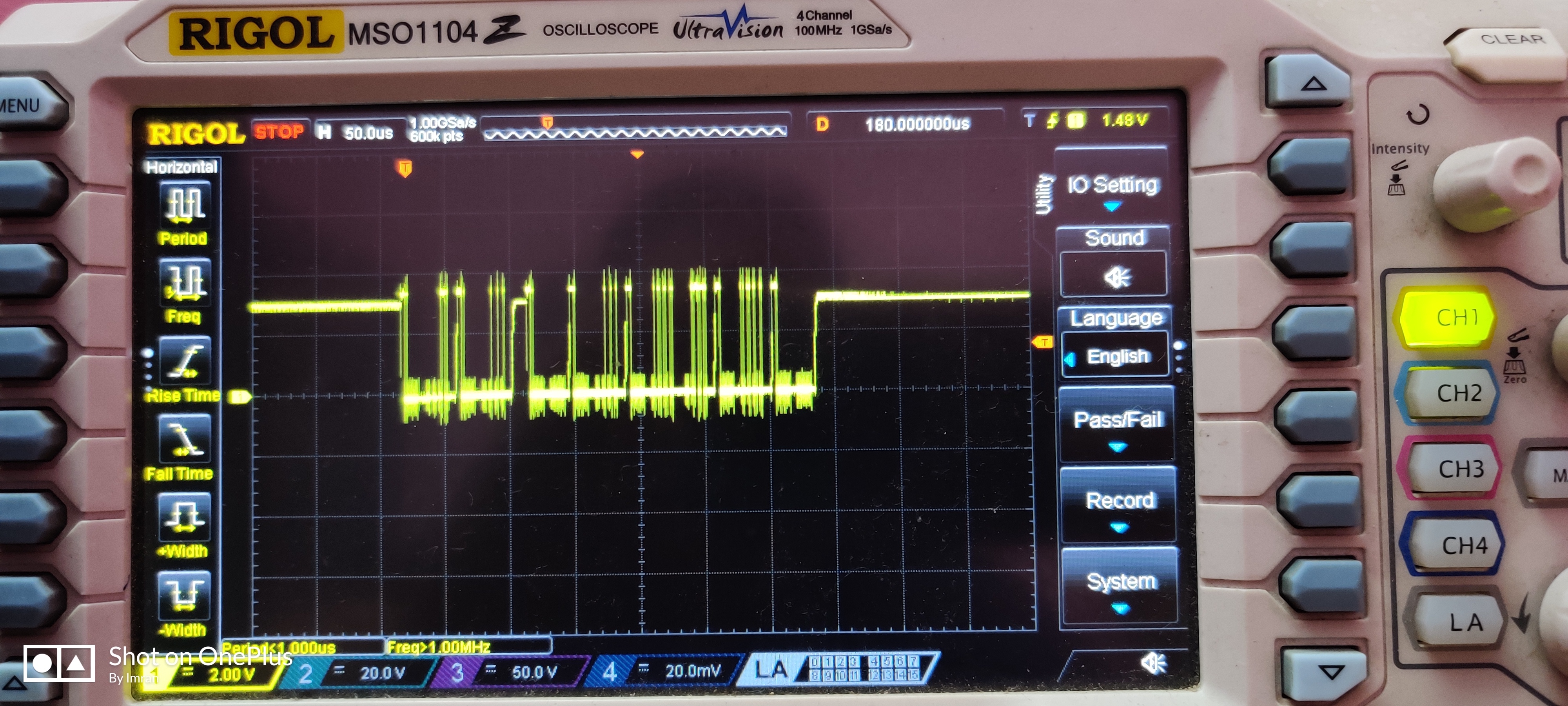
I am not able to read the register from SPI.
when I am trying to read the register it returning 0xffffffff.
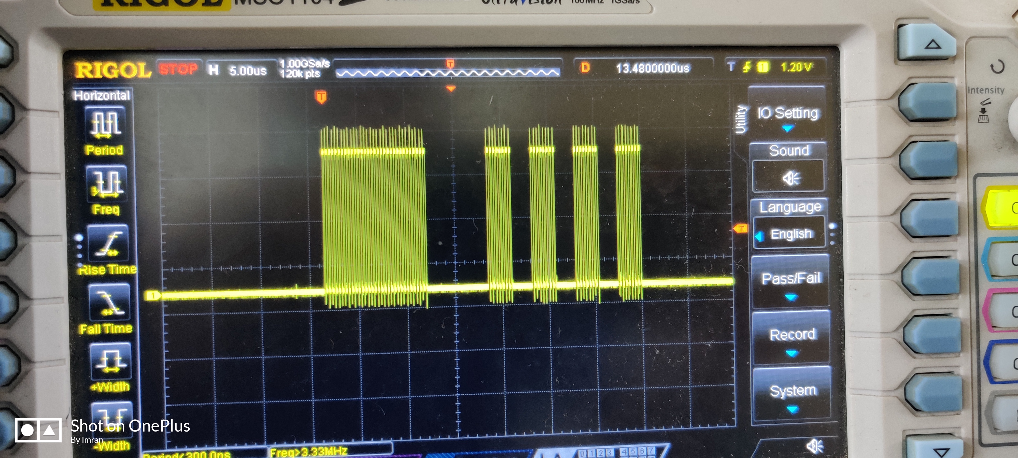
What I am getting on hardware
VSUP Pin 24v
VIO Pin 3.3v
VCCOUT Pin 5V (for aprox 5 min after then 0 volt)
GND 0v
INH Pin left floating
WAKE Pin 24v
FLTR Pin floating
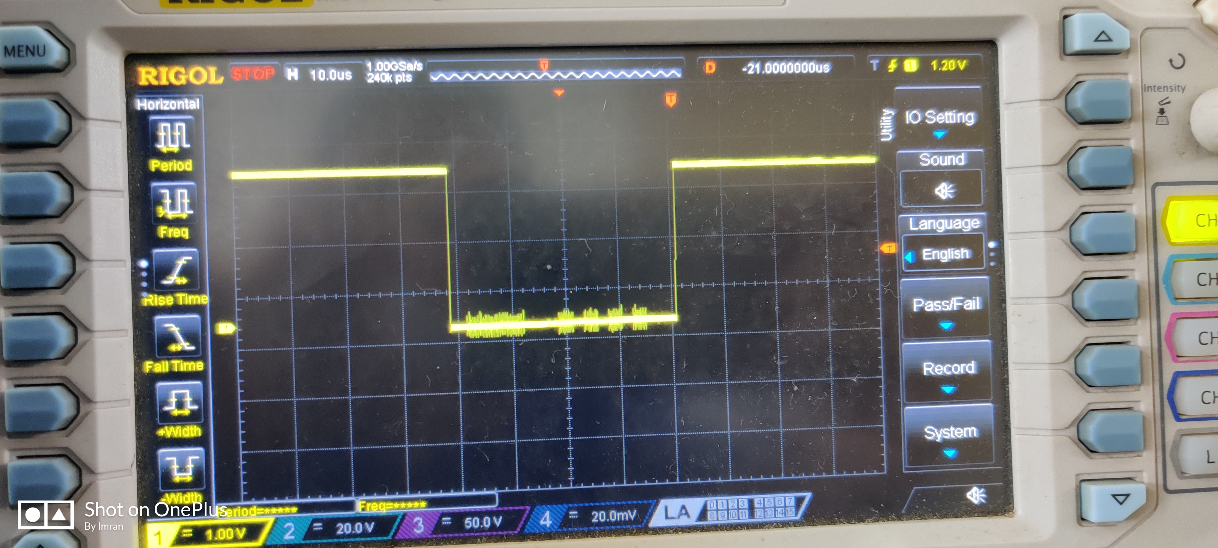
RST Pin pull down
OSC1 and OSC2 Pins 40 MHz clock (for 5 min after it becomes 0 volt)
nWKRQ Pin 0V for aprox 5 min then 3.3v
nINT Interrupt Pin 0V for aprox 5 min then 3.3v
GPO1 Pin 3.3v
GPO2 Pin floating
CANH and CANL Bus Pins 0 volt
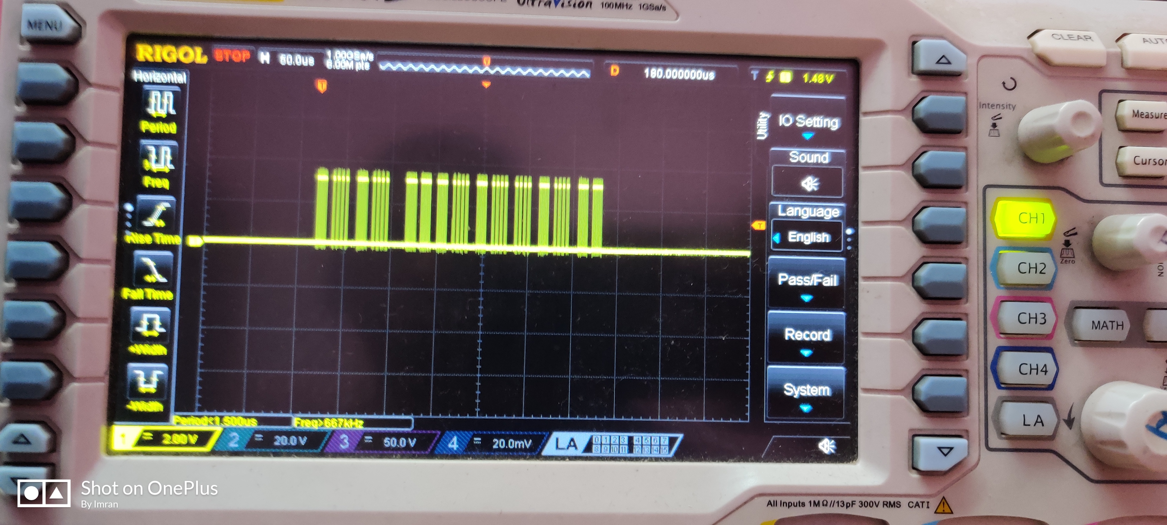
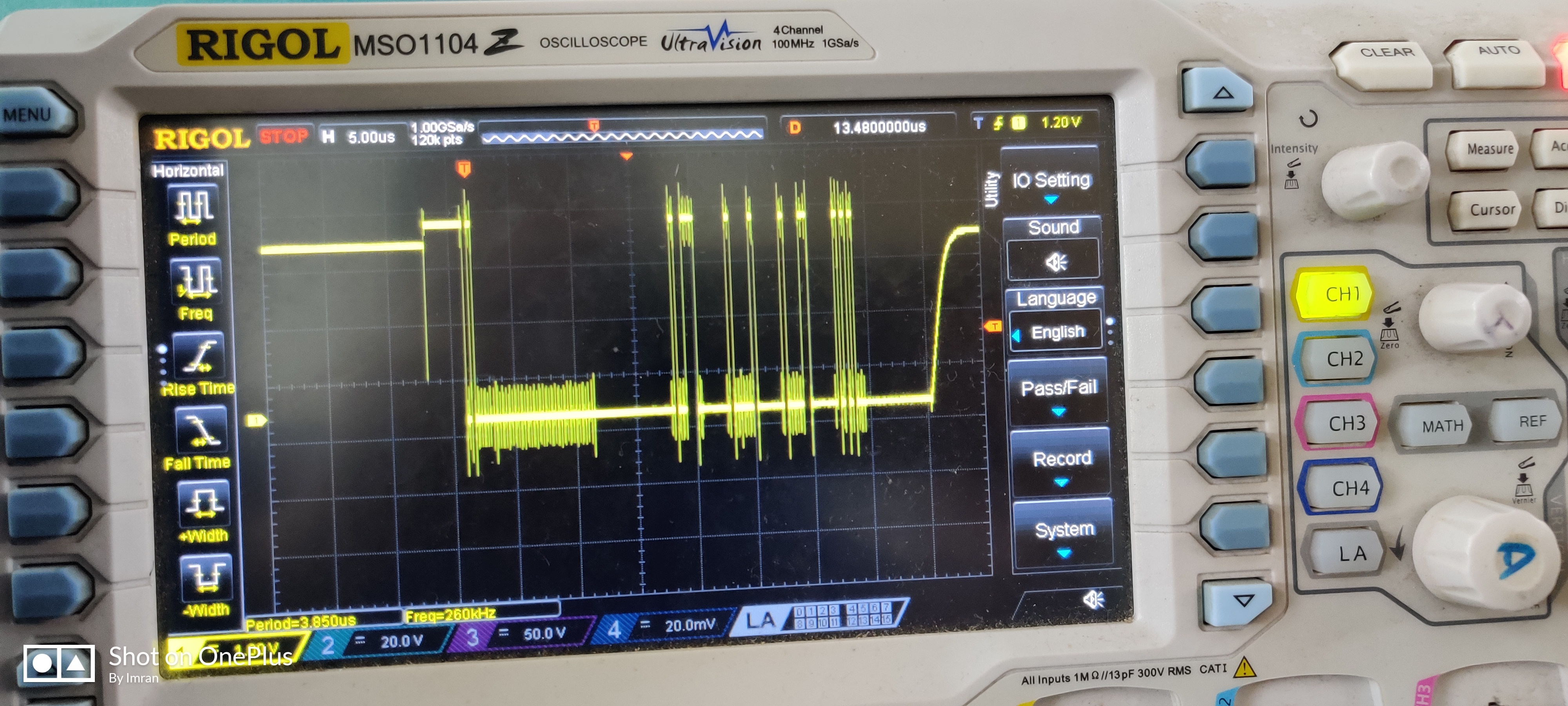
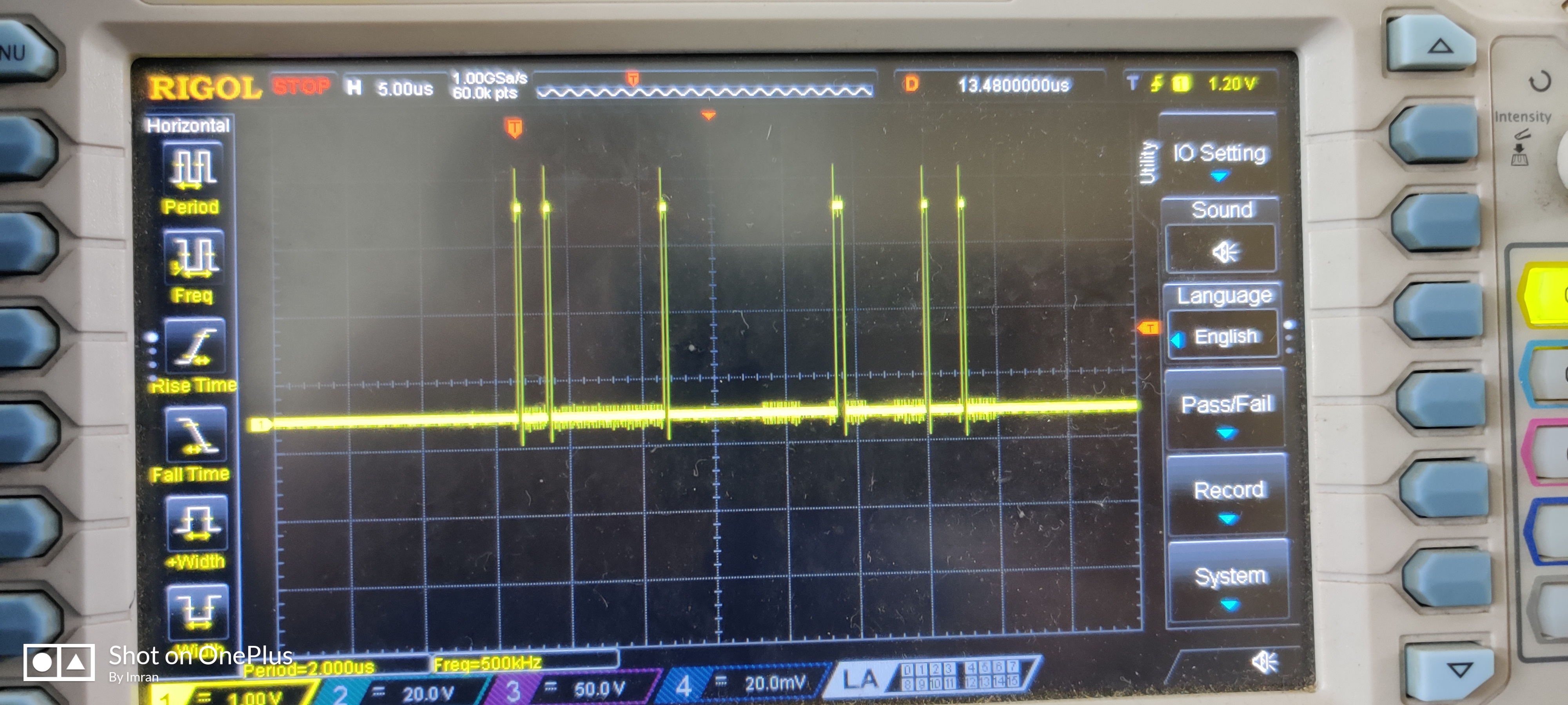
SDO external pull up (3.3 v)
SCK external pull up (0 volt)
SDI external pull up (0 volt)
In code:
SPI data format
1 frame data length 8 bit
MSB first
I have just written a code to read register
I have written the code on the basis of code example given on TI's website
MX_SPI2_Init(); // initialize SPI
spi2_tx=0x41; // read opcode
HAL_GPIO_WritePin(GPIOB, GPIO_PIN_12, GPIO_PIN_RESET); //chip select low
HAL_SPI_Transmit(&hspi2, &spi2_tx, 1, 5); //transmit read opcode
while(HAL_SPI_GetState(&hspi2) == HAL_SPI_STATE_BUSY_TX); //wait to transmit data
spi2_tx=0x10;
HAL_SPI_Transmit(&hspi2, &spi2_tx, 1, 5); //transmit address MSB 8 bit
while(HAL_SPI_GetState(&hspi2) == HAL_SPI_STATE_BUSY_TX); //wait to transmit data
spi2_tx=0x18;
HAL_SPI_Transmit(&hspi2, &spi2_tx, 1, 5); //transmit address LSB 8 bit
while(HAL_SPI_GetState(&hspi2) == HAL_SPI_STATE_BUSY_TX); //wait to transmit data
spi2_tx=0x1;
HAL_SPI_Transmit(&hspi2, &spi2_tx, 1, 5); // length of data to be that is 1 word
while(HAL_SPI_GetState(&hspi2) == HAL_SPI_STATE_BUSY_TX); //wait to transmit data
spi2_tx=0x00;
while(HAL_SPI_GetState(&hspi2) == HAL_SPI_STATE_BUSY); //wait until SPI line becomes idle
HAL_SPI_Transmit(&hspi2, &spi2_tx, 1, 5); // transmit 0x00
while(HAL_SPI_GetState(&hspi2) == HAL_SPI_STATE_BUSY); //wait until SPI line becomes idle
HAL_SPI_Receive(&hspi2, &spi2_rx[0], 1, 5); // read 1 byte
HAL_SPI_Transmit(&hspi2, &spi2_tx, 1, 5); // transmit 0x00
while(HAL_SPI_GetState(&hspi2) == HAL_SPI_STATE_BUSY); //wait until SPI line becomes idle
HAL_SPI_Receive(&hspi2, &spi2_rx[1], 1, 5); // read 1 byte
HAL_SPI_Transmit(&hspi2, &spi2_tx, 1, 5); // transmit 0x00
while(HAL_SPI_GetState(&hspi2) == HAL_SPI_STATE_BUSY); //wait until SPI line becomes idle
HAL_SPI_Receive(&hspi2, &spi2_rx[2], 1, 5); // read 1 byte
HAL_SPI_Transmit(&hspi2, &spi2_tx, 1, 5); // transmit 0x00
while(HAL_SPI_GetState(&hspi2) == HAL_SPI_STATE_BUSY); //wait until SPI line becomes idle
HAL_SPI_Receive(&hspi2, &spi2_rx[3], 1, 5); // read 1 byte
HAL_Delay(10);
HAL_GPIO_WritePin(GPIOB, GPIO_PIN_12, GPIO_PIN_SET); //chip select high
Please help me where i am doing mistake.
Regards
Imran Aftab