Part Number: TCA6424A
Other Parts Discussed in Thread: TCA8418
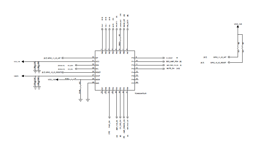
1. VCCI is powered by external LDO, while VCCP is powered by system VSMPS (1.7V). What is the scope of power ripple that VCCI and VCCP need to meet respectively?
2. What is the normal working current and peak current of VCCI and VCCP?
3. Do the power supply of VCCI and VCCP need to be normally turned on? What is the leakage current in the normally turned on state?
4. Are other devices connected to the I2C control line affected?VSMPS (1.7V) is used to pull up the chip end, and the pull up resistance is 2.2K
5, INT and RESET connect to the two GPIO ports of the chip, do you need to pull up resistance, pull up resistance is generally designed for what?
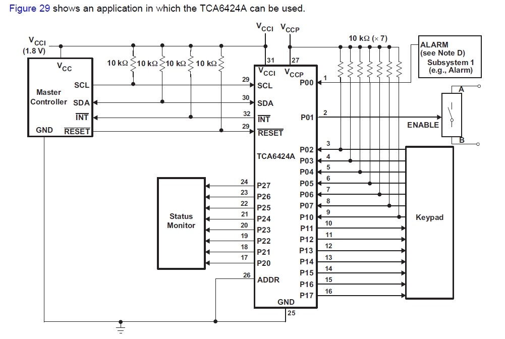
6. When using P00 to P27 for GPIO, can each port be independently configured as input or output, not associated with other ports?When used as input/output, is a pull resistor needed?
7. ADDR generally selects pull up to 1V8 or ground processing by default?