This thread has been locked.

If you have a related question, please click the "Ask a related question" button in the top right corner. The newly created question will be automatically linked to this question.

Compiler/DS90UB926Q-Q1: Pattern Generation of DS90UB926-Q1 and DS90UB936-Q1

Part Number: DS90UB926Q-Q1
Other Parts Discussed in Thread: DS90UB962-Q1, DS90UB936-Q1

Tool/software: TI C/C++ Compiler

Hi TI members:

Our project have one DS90UB962-Q1(on i2c0, address 0x34) & DS90UB936-Q1(on i2c3, address 0x3d)

We already can detect the two chip through i2cdetect tool in kernel. 

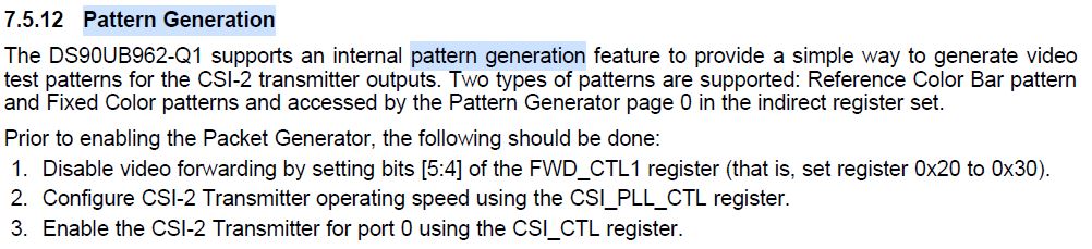
Right now, we are testing the Patteren Generation function on DS90UB962 and DS90UB936, like below picture describe.

I use i2cset tool to configure them.

i2cset -f -y 3 0x34 0x20 0x30
i2cset -f -y 3 0x34 0x1F 0x02
i2cset -f -y 3 0x34 0x33 0x01

But after I configure those register,

there is nothing output form DS90UB962-Q1 CSI0_CLKN and CSI0_D0N, those PINs  are still at low level.

And in DS90UB936 part, I can see the CSI pins be pulled high to 1.8v level, but there is still no data and clock output.

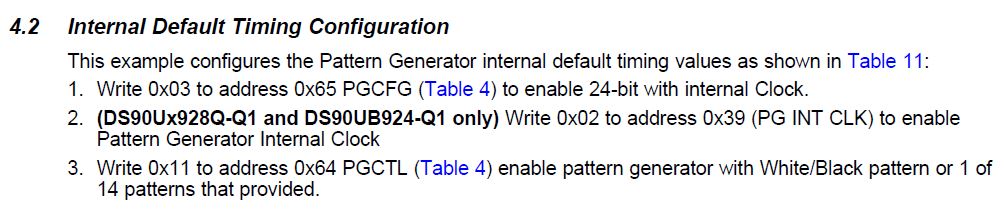
I also try the steps of Internal Default Timing Configuration on snal132e.pdf

Also use i2cset tool, 

i2cset -f -y 3 0x34 0x65 0x03
i2cset -f -y 3 0x34 0x64 0x11

But there is still no output on DS90UB962 CSI pins.

Actually I compare the two registers in DS90UB962 and DS90UB936 datasheet, 

0x64 and 0x65 should be Slave register, 

So I am not sure I should to follow which one pdf file.

Can you help to check this request? 

BR

Sentinen Chen

  • Hello Sentinen,

    The pattern generation manual you are using was written for IVI devices, whereas the 962 and 936 are both ADAS devices. The datasheet for these devices contains the right register information, so disregard the programming of Internal Default Timing in registers 0x65 and 0x64. Those are slave registers on the 962.

    Make sure that your tx speed and lane count are configured correctly for your receiver.

    Pattern generation features on the ADAS and IVI devices are different, so be sure to follow the 962 and 936 datasheets carefully and program the correct registers. Please reference 962 datasheet section 7.5.12.4 and 936 datasheet section 7.5.11.4 for information on programming the indirect access pattern generator registers.

    If in doubt, you can send me your register configuration and I can look it over.

    Regards,

    Carrie

  • Hi Carrie:

    In 936 part, I follow 7.5.11.4 to setup register config, now I can measure some data form CSI pins.

    But in 962 part, I follow 7.5.12.4 to setup, I still can't mesure anything.

    And then I double check 0x33 register in 962. 

    I find 0x33 register in 962 can't be changed.

    after I set 0x01 to 0x33 register in 962, but It is still 0x00 value. 

    I also config other register(0x20) value to confirm i2ctool can work able on 962.

    root@j7-evm:~# i2cget -f -y 3 0x34 0x20
    0xf0
    root@j7-evm:~# i2cget -f -y 5 0x3d 0x1F
    0x02
    root@j7-evm:~# i2cget -f -y 5 0x3d 0x33
    0x00
    root@j7-evm:~# i2cset -f -y 3 0x34 0x20 0x30
    root@j7-evm:~# i2cset -f -y 3 0x34 0x1F 0x02
    root@j7-evm:~# i2cset -f -y 3 0x34 0x33 0x01
    root@j7-evm:~# i2cget -f -y 3 0x34 0x33
    0x00
    root@j7-evm:~# i2cget -f -y 3 0x34 0x1F
    0x02
    root@j7-evm:~# i2cget -f -y 3 0x34 0x20
    0x30

    I also try to use PDB pin to reset 962 again, but 0x33 register still can't be change. 

    Do you have any idea about this situation? 

    BR

    Sentinen Chen

  • Hello Sentinen,

    On the 962, register 0x33 CSI_CTL is a TX port specific register. To read and write to CSI TX port specific registers, you first have to configure register 0x32 CSI_PORT_SEL. Set register 0x32 to 0x01, and then write to register 0x33.

    Regards,

    Carrie

  • Hi Carrie:

    Thanks a lot!!!

    After config 0x32 CSI_PORT_SEL register, now we can enable CSI_CTL successfully.

    BR

    Sentinen Chen