This thread has been locked.

If you have a related question, please click the "Ask a related question" button in the top right corner. The newly created question will be automatically linked to this question.

TPS65987D: Steps for switching from sink to source

Part Number: TPS65987D
Other Parts Discussed in Thread: MSP430FR2433, BQ25713, TPS5450, EV2400, TPS65987

Hi,

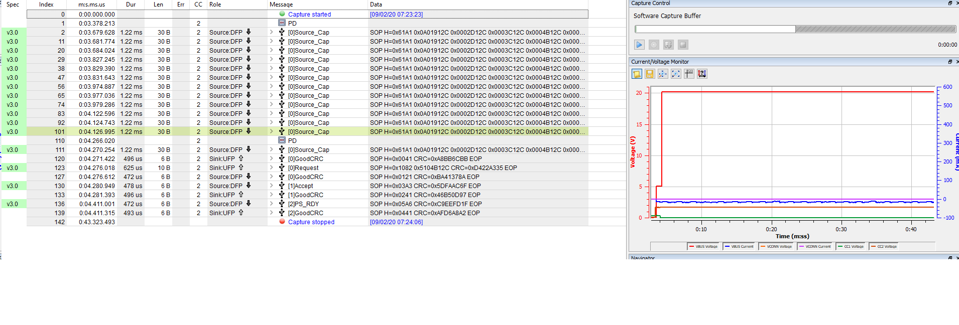
I need to switch a port that is mostly a battery charge sink to a source so that we can use OTG type devices.  I've played around with number of settings and registers but can't seem to get it to switch over.  Can someone summarize the steps and registers required?

I am starting from the default sink project available in the GUI tool.  I setup the transmit source capabilities and asked it to switch over a few different ways. 

5V power is connected on PP_HV1 and 2 and 3.3V is powered from an external LDO. 

Thanks,

Chris

  • Hi Chris,

    You can change the port role by changing the bits 0:1 of the port control register (0x28). Did you experiment with this?

    Setting these bits to 0x01 will change the role to source only.

    Does this answer your question?

    Regards,
    Kedar

  • I did try that.  I actually just found a more detailed doc here, but still having trouble. 

    I wrote this script, but no luck.  Is there a reason the read values are 0 from the first 3 registers?

  • Hi Chris,

    The read should have read the written value. I will need some time to investigate this.

    So, it appears that you want to switch to a source role after you detect and OTC device. The last command you executed (Swap to Source) seems to have returned successfully, but you still see that the device is in a sink role? Can you share the PD logs from a tool such as TotalPhase?

    Regards,
    Kedar

  • I don't have a totalphase analyzer but have ordered one.  The various status registers seem to be indicating some odd and conflicting information. 

  • I should also add that its very unclear which of these registers need to saved to flash and which can be adjusted by writes.  I'm using the writes because most of my flash attempts have failed with any number of indecipherable error messages.  For instance, attempts to change 0x32 never seem to stick.

  • Hi Chris,

    For your previous observation, when the Type-C is not connected and if the port is set as a DRP, you may see conflicting values based on when the individual reads of the registers happen, since the toggle is between SRC and SNK.

    For the last question, I would need to see some logs.

    Did you get the TotalPhase analyzer?

    Please share the PD logs from TotalPhase and I2C logs for further investigation.

    Regards,
    Kedar

  • Kedar, this kind of troubleshooting is just painfully slow.  Can we do a screenshare debug session so I can hope to get somewhere soon?  Otherwise I'm going to need to choose another vendor as I just can't afford this huge delay on the project. 

    I have a total phase analyzer.  And can look at the bus messages, but right now I can't even get the TPS chip to put 5V on the bus so that the messaging can start to happen. 

    I am having a lot of trouble with registers that I set and the values never change.  Flash appears to finally be getting good verification but when I examine registers in debug mode they are not as setup. 

    C

  • Hi Chris,

    Yes we can have a debug session. But before that, could you share the logs I requested? I suspect there may be something with the setup that's causing this.

    I presume you are using our EVM to run your tests.

    Is my understanding correct?

    For the debug session, I would require:

    1. Aardvark I2C/SPI analyzer,
    2. TPS65987D EVM + your platform.
    3. An Oscilloscope.

    Please confirm you have these with you and we can setup a call for debugging this.

    Regards,
    Kedar

  • At the time the logs I shared were everything I had.  The PD Analyzer wasn't displaying anything because there were no messages being sent.  I've since made some further progress but still have issues. 

    The TPS chip won't successfully execute an SRDY command no matter what other commands I give to try and alleviate the problem. 

    At the moment I'm only talking to the chip with the App Customization Tool until I can get proper operation.  At that point I'll move the commands to my micro over I2C.

    Anyway, here is the PD state machine trace:

    Port 0 Type-C 0x0 = SRC_STATE_DISABLED

    Port 0 Type-C 0x0 = SRC_STATE_DISABLED

    Port 0 Type-C 0x0 = SRC_STATE_DISABLED

    Port 0 Type-C 0x0 = SRC_STATE_DISABLED

    Port 0 INT 0x51 = READY_FOR_PATCH

    Port 0 PD 0x1 = PEState_CableTypeDetect

    Port 0 Type-C 0x66 = COMMON_STATE_UNATTACHED_SNK

    Port 1 PD 0x1 = PEState_CableTypeDetect

    Port 1 Type-C 0x0 = SRC_STATE_DISABLED

    Port 0 Type-C 0x65 = COMMON_STATE_ATTACHWAIT_SNK

    Port 0 Type-C 0x61 = COMMON_STATE_ATTACHED_SNK

    Port 0 BC 1.2 0x0 = CHARGER_DETECTION_INIT

    Port 0 PD 0x2 = PEState_LaunchPolicyEngine

    Port 0 PD 0x21 = PEState_Sink_Startup

    Port 0 VBUS 0xcc = VBUSState_MON_HILO

    Port 0 VBUS 0x90 = VBUSState_MON_HI

    Port 0 PD 0x22 = PEState_Sink_Discovery

    Port 0 PD 0x24 = PEState_Sink_WaitForCapabilities

    Port 0 BC 1.2 0x11 = SECONDARY_DETECTION_WAIT

    Port 0 BC 1.2 0xe = CHARGER_DETECTION_DISABLED

    Port 0 Protocol 0xc0 = PRState_SQUELCH_ACTIVE

    Port 0 Protocol 0xc1 = PRState_SQUELCH_IDLE

    Port 0 Protocol 0xc5 = PRState_RX_BUF_RDY

    Port 0 PD 0x26 = PEState_Sink_EvaluateCapability

    Port 0 PD 0x27 = PEState_Sink_SelectCapability

    Port 0 Protocol 0xc8 = PRState_TXDONE

    Port 0 Protocol 0xc0 = PRState_SQUELCH_ACTIVE

    Port 0 Protocol 0xc1 = PRState_SQUELCH_IDLE

    Port 0 Protocol 0xc5 = PRState_RX_BUF_RDY

    Port 0 Protocol 0xcb = PRState_RECEIVED_GOODCRC

    Port 0 Protocol 0xc0 = PRState_SQUELCH_ACTIVE

    Port 0 Protocol 0xc1 = PRState_SQUELCH_IDLE

    Port 0 Protocol 0xc5 = PRState_RX_BUF_RDY

    Port 0 PD 0x28 = PEState_Sink_TransitionSink

    Port 0 BC 1.2 0x2 = PRIMARY_DETECTION

    Port 0 BC 1.2 0xf = PRIMARY_DETECTION_WAIT

    Port 0 BC 1.2 0x10 = DISABLE_PRIMARY_DETECTION_WAIT

    Port 0 BC 1.2 0x3 = SECONDARY_DETECTION

    Port 0 BC 1.2 0x4 = CHARGER_DETECTION_COMPLETE

    Port 0 Protocol 0xc0 = PRState_SQUELCH_ACTIVE

    Port 0 Protocol 0xc1 = PRState_SQUELCH_IDLE

    Port 0 Protocol 0xc5 = PRState_RX_BUF_RDY

    Port 0 PD 0x29 = PEState_Sink_TransitionSink_PS_RDY

    Port 0 PD 0x2a = PEState_Sink_Ready

    And here is a screenshoot of the PD analyzer trace:

    I do have all the other equipment for debug.  Please let me know when you are available.

    Thanks,

    Chris

  • Hi Chris,

    I will send you a personal message regarding the meeting proposal.

    Regards,
    Kedar

  • Thanks for the call and supporting the ongoing work on this project.  As you know we still don't have all the problem solved but identified a few issues with the EVM tools.  I'll try to summarize here for archival purposes and to potentially kick off a separate resolution on those areas. 

    I'm using the following chips:

    - MSP430FR2433 as the I2C master

    - TPS65987D as the USB-C interface

    - BQ25713 battery charger

    - BQ40Z50-R3 as the fuel gauge

    - TPS5450 as a 5V buck

    I have Qty 3 18650 type cells in series and a variety of loads at 9V and 5V.  Right now I have EVM boards for each of those products wired up together. 

    Debugging has been a major challenge as it seems the EVM tools often don't like to work in concert with each other.  Here are some of the issues:

    - FTDI USB interface and drivers are inconsistent and problematic.  I've seen where a simple I2C scan won't even start with a "Exception Encountered during I2C Address Sweep:No FTDI I2C channels (I2C_GetNumChannels) detected, exiting...." message shows up.  After a combination of power cycles, USB cable unplug/replug, shutting everything else down, or removing all other USB devices, etc I can sometimes get it to work.

    - Error messages from the TPS GUI are not very useful.  When you're debugging a complicated system and are faced with a variety of problems having useful error messages is essential.  I've seen problems with everything from flash program verify errors, simple chip not responding to I2C read, config registers not taking write operations even though the GUI implies they were successful, and general I2C issues.  Some of this may have been due to errors on my part but having a useful error message really helps getting to the bottom of the root issue and accelerating the development.

    - I2C tools need to support multi-master on bus.  The GUI tools can be really useful but if you are developing anything but the simplest system they will need to work with other devices too.  Right now I have a complicated scheme where I need to remove the EVM from the rest of the system just to connect the GUI long enough to read some special register or issue a command.  Pull-up resistors on various boards can make this complicated too. 

    - EV2400 (interface to the charger and fuel gauge) seems to often disconnect.  I've had to make sure its the only USB device plugged in when running a long battery test.

    - EVMs should have two I2C connectors so devices can be easily bused together or bypassed

    - More test points needed.  3.3V power on the TPS EVM needs to be brought out to a test point (both VIN_3V3 and LDO_3V3).  CC lines and USB_P/N too.

    - Not all chips behave the same on the I2C bus when un-powered (BQ25713).  This makes a complicated mess of trying to communicate to chips in some configs but a dormant chip bringing the whole bus down.  I've remedied this with the right combination of series resistors and pull-ups, but that's a bit of a band-aid.

    I guess one common theme is an I2C bus tool that is robust, mature, flexible, consistent, and open source would certainly be nice and fix many issues above.  Potentially something like the MSP chip inside the EV2400 could be a common interface supported on all EVMs. 

    Hope that helps your team understand the typical issues.

    C

  • I spoke with Kedar on the phone.  It seemed like by starting from a sink TPS65987 project and making the following changes we could get it to sink or source power. 

    • Port config to DRP
    • Add at least one transmit source PDO with 5V.
    • Set PP1 to source or sink in the global sys config.
    • Ensure the 20V PDO is in the transmit sink PDO list. 

    My issue now is that when I program the flash and try to reproduce the results above many of the config registers are not as we had just set in flash and therefore the system doesn't work.  Sometimes the flash verification does fail in previous step.

    I have also previously moved R40 to R43 as this is the MISO pull down resistor which seemed to be needed to get LDO_3v3 to power up when the battery was dead.  I am also back driving this net with 3V3 from another regulator derived from battery voltage, but that's not always available. 

  • Hi Chris,

    Can you please share a screenshot of the Boot flags in debug mode?

    This tells whether a flash boot was successful or not. Also, Can you confirm the "Version" register in the debug mode shows the correct patch version?

    Regards,
    Kedar

  • The boot flags seem to be inconsistent.  Sometime they say one thing and other times another.  I adjusted the boot resistors so that they use 0.3 to 0.38 ADCIN1 value, or Dead battery mode BP_ECWait_internal and Device Config Infinite Wait.  Is there a way to confirm those settings were properly loaded?  Do you agree they are the best choice in my application?

  • Hi Chris.

    The below highlighted comparison doesn't look right to me. The filed highlighted should be "true".

    Can you confirm under what circumstances the SPI flash doesn't get detected?

    Regards,
    Kedar

  • There is no screen shot or other file in your previous post.

  • It seems the difference is based on whether the USB-C cable is plugged in or not.  Keep in mind I am powering LDO_3V3 from a separate source so that cable shouldn't be needed.  In fact in many cases I would like the device to act as a USB source and their will not be a USB cable plugged in initially. 

    Why does the flash only get loaded when USB-C is plugged in?  How can I power the device and configure it so that startup is always the same? 

  • I should add that when my battery really is dead I will need the 3.3V from the TPS to supply a small amount of current to other system components (MSP430) in order to get the battery charge sequencing up and running. 

    I used LDO_3V3 for this purpose and others above, but seems that may not work.  How should I resolve this?  I don't think I can tie LDO_3V3 and VIN_3V3 together.  Perhaps a well placed schottky diode somewhere? 

  • Hi Chris,

    I am taking over for Kedar, who has brought me up to speed on your issues. On your side, can you check that the EEPROM's voltage is stable?

    Also, the allowable external load on the LDO_3V3 pin is 25mA so I would say that this will not be able to provide your system power in the case of a dead battery. Keep in mind that VIN_3V3 and LDO_3V3 are already connected internally in the TPS65987D. What are your other options for this?

    Regards,

    Emma

  • Emma, great to meet you.

    The power I need for my controller is just a few mA so I think we're good there.  When I measure the voltage I get a consistent 3.27V so I don't think its a question of overloading things. 

    I've played with different configurations and whenever the USB is not plugged in it always says SPI Flash Present = False.  What do I need to do to get it to recognize this flash when the USB is NOT plugged in?

    Once I have answered that I can adjust where the power comes from in the different situations. 

    C

  • Hi Chris,

    The reason I ask about the voltage is that if it drops at all, the SPI flash would not be recognized by the PD controller. Do you get a constant voltage measurement of 3.3V?

    Also, what exactly are you plugging in, and does the SPI flash regularly show up once it is plugged in and not show up when it is not plugged in?

    Regards,

    Emma

  • I do have a constant voltage measurement on my o-scope. 

    I just plug a USB PD charger in.  When I stay the flash is not there I'm referring to the boot flag register.  I have often executed a cold reboot command to see if the status changes but it does not.  I have also removed and reconnected the 3.3V power. 

  • Hi Chris,

    Can you attach a picture of the 3.3V measurement from your scope?

    Regards,

    Emma

  • Played around with the system a bit more and found a few interesting things. 

    1. SPI flash present is false whenever you re-boot from a cold reboot command.  Not sure why but that significantly confused things.  I have about 3 to 4 cables to unplug to ensure all power to eval board is gone so I thought that was a good testing technique.  No idea why, but apparently needs a real full power cycle re-boot.

    2. I added a small diode from LDO_3V3 to Vin_3V3 and now things appear to work fine.  Dead battery startup is good.  Charging is good.  OTG output is good. If the power is always small (<25mA) do you see any problem with this setup?

    Thanks,

    Chris

  • Hi Chris,

    So just to clarify, the diode was able to fully resolve your problems?

    Thanks,

    Emma

  • It seems it has but I'm still running the system through all the various modes that it needs to properly work in. 

    But I'm wondering if you see any potential issues which may arise that I haven't considered or tested?

  • Hi Chris,

    I'm glad everything is working, however, you shouldn't need a diode between the two. A diode won't hurt anything. If you are back feeding LDO_3V3, you should consider resolving that in the hardware, however. I can take a look at your schematic if you need guidance on that. 

    Regards,

    Emma

  • The diode is the "hardware" solution because I need power to flow both ways from Vin_3V3 and from LDO_3V3 in different circumstances.  I can share the schematic via private message.

  • Hi Chris,

    Please keep in mind that LDO_3V3 should really only be used as an output, and VIN_3V3 as an input. If the diode is allowing that to happen, then that will be a good work around. I am going to go ahead and close this ticket, as your issue is solved. If you would like me to view your schematic, please send it over. You can reopen this ticket or submit a new one if other issues arise. 

    Regards,

    Emma