This thread has been locked.

If you have a related question, please click the "Ask a related question" button in the top right corner. The newly created question will be automatically linked to this question.

SN75LVDS83: Δ|VOD|

Part Number: SN75LVDS83

Hi team,

Let me ask you general basic question regarding LVDS spec.

Many datasheet shows that Δ|VOD| "Change in the steady-state differential output voltage magnitude between opposite binary state".

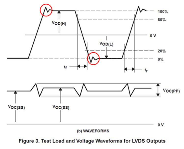
What does it stand for in Figure.3 waveform?

Is it deviation from target amplitude as circled with RED in below?

Best regards,

Shota Mago

  • Hi Shota,

    Normally, the waveform should be flat if the test condition is good. The figure 3 diagram illustrates the potential noise could be coupling in. We specified the differential output voltage on almost all LVDS products and driven by the Voc. The ripple or overshoot voltage circled in red is normally due to how much you can control and minimize the impedance matching. For example the discontinuity due to the via then it introduce the reflection and appear on the red circle. It can be also coming from parasitic capacitance.

    Hope this helps. Let me know if you have further questions.

    Aaron

  • Hi Aaron,

    Thanks for your quick reply and explanation for the waveform.

    Could you simply explain definition of ∆|VOD| (Change in the steady-state differential output voltage magnitude between opposite binary states) ?

    Does it mean just difference of amplitude at steady state between H and L(∆|VOD|=|Vod(H)-Vod(L)|)?

    Best regards,

    Shota Mago

  • Hi Shota,

    Your thinking is correct.

    Aaron