This thread has been locked.

If you have a related question, please click the "Ask a related question" button in the top right corner. The newly created question will be automatically linked to this question.

Compiler/DS90UB962-Q1: Indirect Access reserved register about DS90UB962

Part Number: DS90UB962-Q1
Other Parts Discussed in Thread: DS90UB960-Q1,

Tool/software: TI C/C++ Compiler

Hi TI Members:

I study the  imx390_cfg.h which in PSDKRA_06_02/vision_apps/utils/sensors/src and DS90UB960-Q1 Datasheet now, 

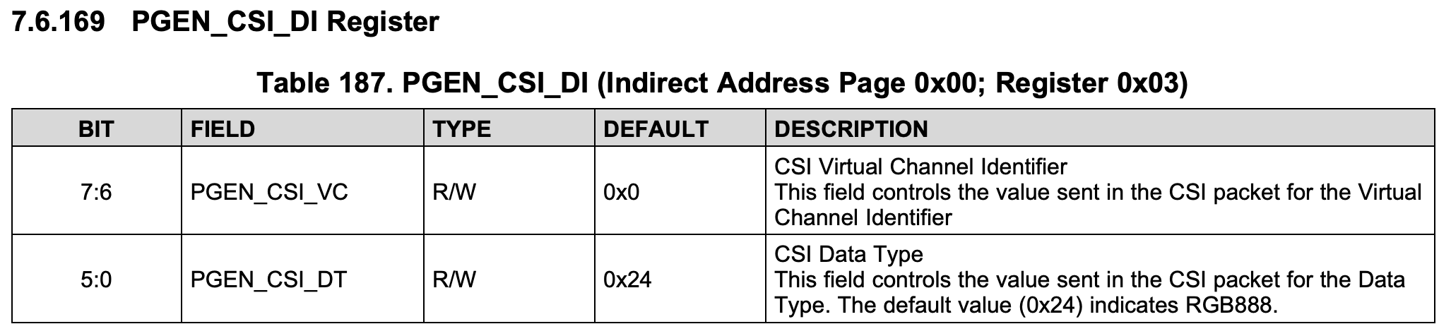
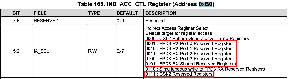
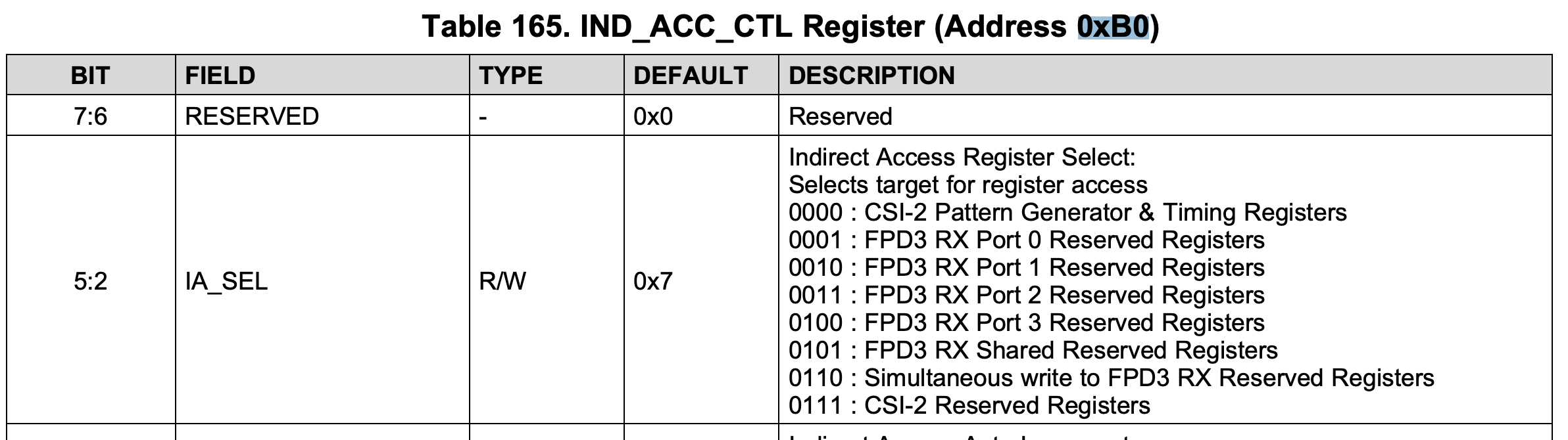
I found there is a lot of register control at 0xB0's related reserved register, like below.

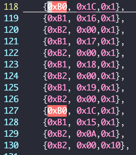
But after I compare DS90UB960-Q1 Datasheet,

There is no related describe about another reserved register, except 0000 : CSI-2 Pattern Generator & Timing Registers target,

Because we are trying to init  DS90UB962, but there is the some problem in DS90UB962-Q1 Datasheet.

Do you know where we can get related register descible? 

BR

Sentinen Chen

  • Hello Sentinen,

    these registers needed to be written only in earlier samples of this device, but since it is already released to production (3 years ago), you do not need to write these registers.

  • Hi Hamzeh:

    Thanks your reply, 

    because we still on debug the UB936 pattern generation function. 

    Can you still provide us the detailed value describe of UB936's indirect Access Register 0x03 (PGEN_CSI_DI),

    right now I only know 0x2B is RAW10, 0x24 is RGB888, 

    I need a detail value list.

    BR

    Sentinen Chen 


  • Hello Sentinen,

    you can find all the Pattern Generator relevant registers in the UB936 datasheet, in section "7.6.165 Indirect Access Registers"

  • Hi Hamzeh:

    Sorry, I am not sure the document we see are the same file.

    Form the UB936 datasheet I download 2502.ds90ub936-q1.pdf, there is only register and default value describe, like below picture.

    As I described, I need the detailed value to know the relationship between the register value and Data type. 

    BR

    Sentinen Chen

  • Hello Sentinen,

    Sorry but we do not have the rights to provide these details. These details are part of the MIPI CSI-2 specification standard and can be found on those documentations.

  • Hi Hamzeh:

    Sorry to brother you again.

    As our work recetly, we can get capture data form UB962's CSIRX0 part,

    But we find there are some important register still need us to control, 

    Below part is one of those registers control flow:

    {0xB0, 0x1C, 0x1}
    {0xB1, 0x15, 0x1}
    {0xB2, 0x0A, 0x1}
    {0xB2, 0x00, 0x1}

    The situation is not like your describe that we do not need to write these register, 

    Can you provide us those registers detail describle? 

    BR

    Sentinen Chen

  • Hello Sentinen,

    Believe me you do not need to set any of those registers! These are not public registers and should not be used by our customers. These are just for internal use.

    Can you tell me what is the importance of setting these registers?

  • Hi Hamzeh:

    Just like my eariler post,

    {0xB0, 0x1C, 0x1}
    {0xB1, 0x15, 0x1}
    {0xB2, 0x0A, 0x1}
    {0xB2, 0x00, 0x1}

    If I didn't enter value 0x0A --> 0x00 to 0x15 register,

    then I can't see the UB962 start to transfer CAMERA data on CSI datalanes.

    PS:

    I was follow RTOS pdk code that Board_FpdUb960CfgObj config on pdk/packages/ti/board/src/devices/fpd/ds90ub960.c 

    /******************************************************************************
     * Copyright (c) 2019 Texas Instruments Incorporated - http://www.ti.com
     *
     *  Redistribution and use in source and binary forms, with or without
     *  modification, are permitted provided that the following conditions
     *  are met:
     *
     *    Redistributions of source code must retain the above copyright
     *    notice, this list of conditions and the following disclaimer.
     *
     *    Redistributions in binary form must reproduce the above copyright
     *    notice, this list of conditions and the following disclaimer in the
     *    documentation and/or other materials provided with the
     *    distribution.
     *
     *    Neither the name of Texas Instruments Incorporated nor the names of
     *    its contributors may be used to endorse or promote products derived
     *    from this software without specific prior written permission.
     *
     *  THIS SOFTWARE IS PROVIDED BY THE COPYRIGHT HOLDERS AND CONTRIBUTORS
     *  "AS IS" AND ANY EXPRESS OR IMPLIED WARRANTIES, INCLUDING, BUT NOT
     *  LIMITED TO, THE IMPLIED WARRANTIES OF MERCHANTABILITY AND FITNESS FOR
     *  A PARTICULAR PURPOSE ARE DISCLAIMED. IN NO EVENT SHALL THE COPYRIGHT
     *  OWNER OR CONTRIBUTORS BE LIABLE FOR ANY DIRECT, INDIRECT, INCIDENTAL,
     *  SPECIAL, EXEMPLARY, OR CONSEQUENTIAL DAMAGES (INCLUDING, BUT NOT
     *  LIMITED TO, PROCUREMENT OF SUBSTITUTE GOODS OR SERVICES; LOSS OF USE,
     *  DATA, OR PROFITS; OR BUSINESS INTERRUPTION) HOWEVER CAUSED AND ON ANY
     *  THEORY OF LIABILITY, WHETHER IN CONTRACT, STRICT LIABILITY, OR TORT
     *  (INCLUDING NEGLIGENCE OR OTHERWISE) ARISING IN ANY WAY OUT OF THE USE
     *  OF THIS SOFTWARE, EVEN IF ADVISED OF THE POSSIBILITY OF SUCH DAMAGE.
     *
     *****************************************************************************/
    
    /**
     * \file  ds90ub960.c
     *
     * \brief This file contains the API's for configuring the ds90ub960 deserailizer.
     *
     */
    #include "ds90ub960.h"
    
    /* DES UB960 configurations for RGB888 1280x720 30fps */
    Board_I2cRegProgObj Board_FpdUb960PGCfg0[] =
    {
        {0x32, 0x01, 0x1},   /* Select Port0 registers */
        {0xB0, 0x00, 0x1},   /* Indirect Pattern Gen Registers */
        {0xB1, 0x01, 0x1},   /* PGEN_CTL */
        {0xB2, 0x01, 0x1},
        {0xB1, 0x02, 0x1},   /* PGEN_CFG */
        {0xB2, 0x33, 0x1},
        {0xB1, 0x03, 0x1},   /* PGEN_CSI_DI */
        {0xB2, 0x24, 0x1},
        {0xB1, 0x04, 0x1},   /* PGEN_LINE_SIZE1 */
        {0xB2, 0x0F, 0x1},
        {0xB1, 0x05, 0x1},   /* PGEN_LINE_SIZE0 */
        {0xB2, 0x00, 0x1},
        {0xB1, 0x06, 0x1},   /* PGEN_BAR_SIZE1 */
        {0xB2, 0x01, 0x1},
        {0xB1, 0x07, 0x1},   /* PGEN_BAR_SIZE0 */
        {0xB2, 0xE0, 0x1},
        {0xB1, 0x08, 0x1},   /* PGEN_ACT_LPF1 */
        {0xB2, 0x02, 0x1},
        {0xB1, 0x09, 0x1},   /* PGEN_ACT_LPF0 */
        {0xB2, 0xD0, 0x1},
        {0xB1, 0x0A, 0x1},   /* PGEN_TOT_LPF1 */
        {0xB2, 0x04, 0x1},
        {0xB1, 0x0B, 0x1},   /* PGEN_TOT_LPF0 */
        {0xB2, 0x1A, 0x1},
        {0xB1, 0x0C, 0x1},   /* PGEN_LINE_PD1 */
        {0xB2, 0x0C, 0x1},
        {0xB1, 0x0D, 0x1},   /* PGEN_LINE_PD0 */
        {0xB2, 0x67, 0x1},
        {0xB1, 0x0E, 0x1},   /* PGEN_VBP */
        {0xB2, 0x21, 0x1},
        {0xB1, 0x0F, 0x1},   /* PGEN_VFP */
        {0xB2, 0x0A, 0x1},
        {0x33, 0x01, 0x1},   /* CSI0 enable */
        {BOARD_DEVICES_CONFIG_END},
    };
    
    /* DES UB960 configurations for RGB888 1920x1080 30fps */
    Board_I2cRegProgObj Board_FpdUb960PGCfg1[] =
    {
        {0x32, 0x01, 0x1},   /* Select Port0 registers */
        {0xB0, 0x00, 0x1},   /* Indirect Pattern Gen Registers */
        {0xB1, 0x01, 0x1},   /* PGEN_CTL */
        {0xB2, 0x01, 0x1},
        {0xB1, 0x02, 0x1},   /* PGEN_CFG */
        {0xB2, 0x33, 0x1},
        {0xB1, 0x03, 0x1},   /* PGEN_CSI_DI */
        {0xB2, 0x24, 0x1},
        {0xB1, 0x04, 0x1},   /* PGEN_LINE_SIZE1 */
        {0xB2, 0x16, 0x1},
        {0xB1, 0x05, 0x1},   /* PGEN_LINE_SIZE0 */
        {0xB2, 0x80, 0x1},
        {0xB1, 0x06, 0x1},   /* PGEN_BAR_SIZE1 */
        {0xB2, 0x02, 0x1},
        {0xB1, 0x07, 0x1},   /* PGEN_BAR_SIZE0 */
        {0xB2, 0xD0, 0x1},
        {0xB1, 0x08, 0x1},   /* PGEN_ACT_LPF1 */
        {0xB2, 0x04, 0x1},
        {0xB1, 0x09, 0x1},   /* PGEN_ACT_LPF0 */
        {0xB2, 0x38, 0x1},
        {0xB1, 0x0A, 0x1},   /* PGEN_TOT_LPF1 */
        {0xB2, 0x07, 0x1},
        {0xB1, 0x0B, 0x1},   /* PGEN_TOT_LPF0 */
        {0xB2, 0x08, 0x1},
        {0xB1, 0x0C, 0x1},   /* PGEN_LINE_PD1 */
        {0xB2, 0x06, 0x1},
        {0xB1, 0x0D, 0x1},   /* PGEN_LINE_PD0 */
        {0xB2, 0x33, 0x1},
        {0xB1, 0x0E, 0x1},   /* PGEN_VBP */
        {0xB2, 0x28, 0x1},
        {0xB1, 0x0F, 0x1},   /* PGEN_VFP */
        {0xB2, 0x0F, 0x1},
        {0x33, 0x01, 0x1},   /* CSI0 enable */
        {BOARD_DEVICES_CONFIG_END},
    };
    
    /* DES UB960 configurations for single channel RGB888 1920x1080 30fps
       from UB953 */
    Board_I2cRegProgObj Board_FpdUb960Ub953PGCfg0[] =
    {
        {0x01, 0x02, 0x100},
        {0x1f, 0x00, 0x1},
    
        {0xB0, 0x1C, 0x1},
        {0xB1, 0x16, 0x1},
        {0xB2, 0x00, 0x1},
        {0xB1, 0x17, 0x1},
        {0xB2, 0x00, 0x1},
        {0xB1, 0x18, 0x1},
        {0xB2, 0x00, 0x1},
        {0xB1, 0x19, 0x1},
        {0xB2, 0x00, 0x1},
        {0xB0, 0x1C, 0x1},
        {0xB1, 0x15, 0x1},
        {0xB2, 0x0A, 0x1},
        {0xB2, 0x00, 0x1},
    
        {0x0D, 0x90, 0x1}, /*I/O to 3V3 - Options not valid with datashee*/
        {0x0C, 0x0F, 0x1}, /*Enable All ports*/
    
        /*Select Channel 0*/
        {0x4C, 0x01, 0x1},
        {0x58, 0x5D, 0x1}, /*Enable Back channel, set to 50Mbs*/
        {0x72, 0x00, 0x1}, /*VC map*/
    
        /*Select Channel 1*/
        {0x4C, 0x12, 0x1},
        {0x58, 0x5D, 0x1},/*Enable Back channel, set to 50Mbs*/
    
        /*Select Channel 2*/
        {0x4C, 0x24, 0x1},
        {0x58, 0x5D, 0x1},/*Enable Back channel, set to 50Mbs*/
    
        /*Select Channel 3*/
        {0x4C, 0x38, 0x1},
        {0x58, 0x5D, 0x1},/*Enable Back channel, set to 50Mbs*/
    
        /*Select Channel 0*/
        {0x4C, 0x01, 0x1},
        {0xB0, 0x04, 0x1},
        {0xB1, 0x03, 0x1},
        {0xB2, 0x20, 0x1},
        {0xB1, 0x13, 0x1},
        {0xB2, 0x20, 0x1},
        {0xB0, 0x04, 0x1},
        {0xB1, 0x04, 0x1},
        {0xB2, 0x3F, 0x1},
        {0xB1, 0x14, 0x1},
        {0xB2, 0x3F, 0x1},
        {0x42, 0x71, 0x1}, /*Unknown*/
        {0x41, 0xF0, 0x1}, /*Unknown*/
        {0xB9, 0x18, 0x1},
    
        /*Select Channel 1*/
        {0x4C, 0x12, 0x1},
        {0xB0, 0x08, 0x1},
        {0xB1, 0x03, 0x1},
        {0xB2, 0x20, 0x1},
        {0xB1, 0x13, 0x1},
        {0xB2, 0x20, 0x1},
        {0xB0, 0x08, 0x1},
        {0xB1, 0x04, 0x1},
        {0xB2, 0x3F, 0x1},
        {0xB1, 0x14, 0x1},
        {0xB2, 0x3F, 0x1},
        {0xB0, 0x08, 0x1},
        {0x42, 0x71, 0x1}, /*Unknown*/
        {0x41, 0xF0, 0x1}, /*Unknown*/
        {0xB9, 0x18, 0x1},
    
        /*Select Channel 2*/
        {0x4C, 0x24, 0x1},
        {0xB0, 0x0C, 0x1},
        {0xB1, 0x03, 0x1},
        {0xB2, 0x20, 0x1},
        {0xB1, 0x13, 0x1},
        {0xB2, 0x20, 0x1},
        {0xB0, 0x0C, 0x1},
        {0xB1, 0x04, 0x1},
        {0xB2, 0x3F, 0x1},
        {0xB1, 0x14, 0x1},
        {0xB2, 0x3F, 0x1},
        {0x42, 0x71, 0x1},/*Unknown*/
        {0x41, 0xF0, 0x1},/*Unknown*/
        {0xB9, 0x18, 0x1},
    
        /*Select Channel 3*/
        {0x4C, 0x38, 0x1},
        {0xB0, 0x10, 0x1},
        {0xB1, 0x03, 0x1},
        {0xB2, 0x20, 0x1},
        {0xB1, 0x13, 0x1},
        {0xB2, 0x20, 0x1},
        {0xB0, 0x10, 0x1},
        {0xB1, 0x04, 0x1},
        {0xB2, 0x3F, 0x1},
        {0xB1, 0x14, 0x1},
        {0xB2, 0x3F, 0x1},
        {0x42, 0x71, 0x1},/*Unknown*/
        {0x41, 0xF0, 0x1},/*Unknown*/
        {0xB9, 0x18, 0x1},
    
        {0x32, 0x01, 0x1}, /*Enable TX port 0*/
        {0x20, 0x00, 0x1}, /*Forwarding and using CSIport 0 */
    
        /*Sets GPIOS*/
        {0x10, 0x83, 0x1},
        {0x11, 0xA3, 0x1},
        {0x12, 0xC3, 0x1},
        {0x13, 0xE3, 0x1},
    
        {0x4C,  0x1, 0x1}, /* 0x01 */
        {0x32, 0x01, 0x1}, /*Enable TX port 0*/
        {0x33, 0x02, 0x1}, /*Enable Continuous clock mode and CSI output*/
        {0xBC, 0x00, 0x1}, /*Unknown*/
        {0x5D, 0x30, 0x1}, /*Serializer I2C Address*/
        {0x65, (BOARD_FPD_UB953_PORT_0_SER_ALIAS_ADDR << 1U), 0x1},
        {0x5E, 0x42, 0x1}, /*Sensor I2C Address*/
        {0x66, (BOARD_PORT_0_SENSOR_ALIAS_ADDR << 1U), 0x1},
        {0x6D, 0x6C, 0x1}, /*CSI Mode*/
        {0x72, 0x00, 0x1}, /*VC Map - All to 0 */
        {0x7C, 0x20, 0x10}, /*Line Valid active high, Frame Valid active high*/
        {0xD5, 0xF3, 0x10}, /*Auto Attenuation*/
        {0xB0, 0x1C, 0x1},
        {0xB1, 0x15, 0x1},
        {0xB2, 0x0A, 0x1},
        {0xB2, 0x00, 0x1},
    
        {0x4C, 0x12, 0x1}, /* 0x12 */
        {0x32, 0x01, 0x1}, /*Enable TX port 0*/
        {0x33, 0x02, 0x1}, /*Enable Continuous clock mode and CSI output*/
        {0xBC, 0x00, 0x1}, /*Unknown*/
        {0x5D, 0x30, 0x1}, /*Serializer I2C Address*/
        {0x65, (BOARD_FPD_UB953_PORT_1_SER_ALIAS_ADDR << 1U), 0x1},
        {0x5E, 0x42, 0x1}, /*Sensor I2C Address*/
        {0x66, (BOARD_PORT_1_SENSOR_ALIAS_ADDR << 1U), 0x1},
        {0x6D, 0x6C, 0x1}, /*CSI Mode*/
        {0x72, 0x55, 0x1}, /*VC Map - All to 1 */
        {0x7C, 0x20, 0x10}, /*Line Valid active high, Frame Valid active high*/
        {0xD5, 0xF3, 0x10}, /*Auto Attenuation*/
        {0xB0, 0x1C, 0x1},
        {0xB1, 0x15, 0x1},
        {0xB2, 0x0A, 0x1},
        {0xB2, 0x00, 0x1},
    
        {0x4C, 0x24, 0x1}, /* 0x24 */
        {0x32, 0x01, 0x1}, /*Enable TX port 0*/
        {0x33, 0x02, 0x1}, /*Enable Continuous clock mode and CSI output*/
        {0xBC, 0x00, 0x1}, /*Unknown*/
        {0x5D, 0x30, 0x1}, /*Serializer I2C Address*/
        {0x65, (BOARD_FPD_UB953_PORT_2_SER_ALIAS_ADDR << 1U), 0x1},
        {0x5E, 0x42, 0x1}, /*Sensor I2C Address*/
        {0x66, (BOARD_PORT_2_SENSOR_ALIAS_ADDR << 1U), 0x1},
        {0x6D, 0x6C, 0x1}, /*CSI Mode*/
        {0x72, 0xaa, 0x1}, /*VC Map - All to 2 */
        {0x7C, 0x20, 0x10}, /*Line Valid active high, Frame Valid active high*/
        {0xD5, 0xF3, 0x10}, /*Auto Attenuation*/
        {0xB0, 0x1C, 0x1},
        {0xB1, 0x15, 0x1},
        {0xB2, 0x0A, 0x1},
        {0xB2, 0x00, 0x1},
    
        {0x4C, 0x38, 0x1}, /* 0x38 */
        {0x32, 0x01, 0x1}, /*Enable TX port 0*/
        {0x33, 0x02, 0x1}, /*Enable Continuous clock mode and CSI output*/
        {0xBC, 0x00, 0x1}, /*Unknown*/
        {0x5D, 0x30, 0x1}, /*Serializer I2C Address*/
        {0x65, (BOARD_FPD_UB953_PORT_3_SER_ALIAS_ADDR << 1U), 0x1},
        {0x5E, 0x42, 0x1}, /*Sensor I2C Address*/
        {0x66, (BOARD_PORT_3_SENSOR_ALIAS_ADDR << 1U), 0x1},
        {0x6D, 0x6C, 0x1}, /*CSI Mode*/
        {0x72, 0xFF, 0x1}, /*VC Map - All to 3 */
        {0x7C, 0x20, 0x10}, /*Line Valid active high, Frame Valid active high*/
        {0xD5, 0xF3, 0x10}, /*Auto Attenuation*/
        {0xB0, 0x1C, 0x1},
        {0xB1, 0x15, 0x1},
        {0xB2, 0x0A, 0x1},
        {0xB2, 0x00, 0x1},
        {BOARD_DEVICES_CONFIG_END},
    };
    
    Board_I2cRegProgObj Board_FpdUb960CfgObj[] =
    {
        {0x01, 0x02, 0x100}, /* Digital Rst1 */
        {0x1f, 0x00, 0x1}, /* OSC Clk, Ref Clk, and CSI-2 Tx speed */
    
        {0xB0, 0x1C, 0x1}, /* Indirect Access Register Select:CSI-2 Reserved Registers */
        {0xB1, 0x16, 0x1}, /* Indirect Access Register Address Select: 0x16 */
        {0xB2, 0x00, 0x1}, /* Indirect Access Data Register: 0x00 */
        {0xB1, 0x17, 0x1}, /* Indirect Access Register Address Select: 0x17 */
        {0xB2, 0x00, 0x1}, /* Indirect Access Data Register: 0x00 */
        {0xB1, 0x18, 0x1}, /* Indirect Access Register Address Select: 0x18 */
        {0xB2, 0x00, 0x1}, /* Indirect Access Data Register: 0x00 */
        {0xB1, 0x19, 0x1}, /* Indirect Access Register Address Select: 0x19 */
        {0xB2, 0x00, 0x1}, /* Indirect Access Data Register: 0x00 */
        {0xB0, 0x1C, 0x1}, /* Indirect Access Register Select:CSI-2 Reserved Registers */
        {0xB1, 0x15, 0x1}, /* Indirect Access Register Address Select: 0x15 */
        {0xB2, 0x0A, 0x1}, /* Indirect Access Data Register: 0x0A */
        {0xB2, 0x00, 0x10}, /* Indirect Access Data Register: 0x00 */
        /** I/O to 3V3 - Options not valid with datasheet */
        {0x0D, 0x90, 0x1}, /* SEL3P3V: 3.3V I/O Supply */
        /** Enable All ports */
        {0x0C, 0x0F, 0x1}, /* Recevier Enable for Port-0, Port-1, Port-2, & Port-3 */
    
        /** Select Channel 0 */
        {0x4C, 0x01, 0x1}, /* Write Enable for RX port 0 registers */
        /** Enable Back channel, set to 50Mbs */
        {0x58, 0x5D, 0x1}, /* I2C Pass through enable */
        /** VC map*/
        {0x72, 0x00, 0x1},
    
        /** Select Channel 1 */
        {0x4C, 0x12, 0x1},/* Write & Read Enable for RX port 1 registers */
        /** Enable Back channel, set to 50Mbs */
        {0x58, 0x5D, 0x1}, /* I2C Pass through enable */
    
        /** Select Channel 2 */
        {0x4C, 0x24, 0x1},/* Write & Read Enable for RX port 2 registers */
        /** Enable Back channel, set to 50Mbs */
        {0x58, 0x5D, 0x1}, /* I2C Pass through enable */
    
        /** Select Channel 3*/
        {0x4C, 0x38, 0x1},/* Write & Read Enable for RX port 3 registers */
        /** Enable Back channel, set to 50Mbs */
        {0x58, 0x5D, 0x1}, /* I2C Pass through enable */
    
        /** Select Channel 0 */
        {0x4C, 0x01, 0x1},/* Write Enable for RX port 0 registers */
        {0xB0, 0x04, 0x1},/* Indirect Access Register Select: FPD3 RX Port 0 Reserved Registers */
        {0xB1, 0x03, 0x1},/* Indirect Access Register Address Select: 0x03 */
        {0xB2, 0x20, 0x1},/* Indirect Access Data Register: 0x20 */
        {0xB1, 0x13, 0x1},/* Indirect Access Register Address Select: 0x13 */
        {0xB2, 0x20, 0x1},/* Indirect Access Data Register: 0x20 */
        {0xB0, 0x04, 0x1},/* Indirect Access Register Select: FPD3 RX Port 0 Reserved Registers */
        {0xB1, 0x04, 0x1},/* Indirect Access Register Address Select: 0x04 */
        {0xB2, 0x3F, 0x1},/* Indirect Access Data Register: 0x3F */
        {0xB1, 0x14, 0x1},/* Indirect Access Register Address Select: 0x14 */
        {0xB2, 0x3F, 0x1},/* Indirect Access Data Register: 0x3F */
        {0x42, 0x71, 0x1},
        {0x41, 0xF0, 0x1},
        {0xB9, 0x18, 0x1},
    
        /** Select Channel 1 */
        {0x4C, 0x12, 0x1},
        {0xB0, 0x08, 0x1},/* Indirect Access Register Select: FPD3 RX Port 1 Reserved Registers */
        {0xB1, 0x03, 0x1},/* Indirect Access Register Address Select: 0x03 */
        {0xB2, 0x20, 0x1},/* Indirect Access Data Register: 0x20 */
        {0xB1, 0x13, 0x1},/* Indirect Access Register Address Select: 0x13 */
        {0xB2, 0x20, 0x1},/* Indirect Access Data Register: 0x20 */
        {0xB0, 0x08, 0x1},/* Indirect Access Register Select: FPD3 RX Port 1 Reserved Registers */
        {0xB1, 0x04, 0x1},/* Indirect Access Register Address Select: 0x04 */
        {0xB2, 0x3F, 0x1},/* Indirect Access Data Register: 0x3F */
        {0xB1, 0x14, 0x1},/* Indirect Access Register Address Select: 0x14 */
        {0xB2, 0x3F, 0x1},/* Indirect Access Data Register: 0x3F */
        {0xB0, 0x08, 0x1},/* Indirect Access Register Select: FPD3 RX Port 0 Reserved Registers */
        {0x42, 0x71, 0x1},
        {0x41, 0xF0, 0x1},
        {0xB9, 0x18, 0x1},
    
        /** Select Channel 2 */
        {0x4C, 0x24, 0x1},
        {0xB0, 0x0C, 0x1},/* Indirect Access Register Select: FPD3 RX Port 2 Reserved Registers */
        {0xB1, 0x03, 0x1},/* Indirect Access Register Address Select: 0x03 */
        {0xB2, 0x20, 0x1},/* Indirect Access Data Register: 0x20 */
        {0xB1, 0x13, 0x1},/* Indirect Access Register Address Select: 0x13 */
        {0xB2, 0x20, 0x1},/* Indirect Access Data Register: 0x20 */
        {0xB0, 0x0C, 0x1},/* Indirect Access Register Select: FPD3 RX Port 2 Reserved Registers */
        {0xB1, 0x04, 0x1},/* Indirect Access Register Address Select: 0x04 */
        {0xB2, 0x3F, 0x1},/* Indirect Access Data Register: 0x3F */
        {0xB1, 0x14, 0x1},/* Indirect Access Register Address Select: 0x14 */
        {0xB2, 0x3F, 0x1},/* Indirect Access Data Register: 0x3F */
        {0x42, 0x71, 0x1},
        {0x41, 0xF0, 0x1},
        {0xB9, 0x18, 0x1},
    
        /** Select Channel 3 */
        {0x4C, 0x38, 0x1},
        {0xB0, 0x10, 0x1},/* Indirect Access Register Select: FPD3 RX Port 3 Reserved Registers */
        {0xB1, 0x03, 0x1},/* Indirect Access Register Address Select: 0x03 */
        {0xB2, 0x20, 0x1},/* Indirect Access Data Register: 0x20 */
        {0xB1, 0x13, 0x1},/* Indirect Access Register Address Select: 0x13 */
        {0xB2, 0x20, 0x1},/* Indirect Access Data Register: 0x20 */
        {0xB0, 0x10, 0x1},/* Indirect Access Register Select: FPD3 RX Port 3 Reserved Registers */
        {0xB1, 0x04, 0x1},/* Indirect Access Register Address Select: 0x04 */
        {0xB2, 0x3F, 0x1},/* Indirect Access Data Register: 0x3F */
        {0xB1, 0x14, 0x1},/* Indirect Access Register Address Select: 0x14 */
        {0xB2, 0x3F, 0x1},/* Indirect Access Data Register: 0x3F */
        {0x42, 0x71, 0x1},
        {0x41, 0xF0, 0x1},
        {0xB9, 0x18, 0x1},
    
        /** Enable TX port 0 */
        {0x32, 0x01, 0x1},
        /** Forwarding and using CSIport 0 */
        {0x20, 0x00, 0x1},
    
        /** Sets GPIOS */
        {0x10, 0x83, 0x1},
        {0x11, 0xA3, 0x1},
        {0x12, 0xC3, 0x1},
        {0x13, 0xE3, 0x1},
    
        /** 0x01 */
        {0x4C, 0x01, 0x1},
        /** Enable TX port 0 */
        {0x32, 0x01, 0x1},
        /** Enable Continuous clock mode and CSI output */
        {0x33, 0x02, 0x1},
        {0xBC, 0x00, 0x1},
        /** Serializer I2C Address */
        {0x5D, 0x30, 0x1},
        {0x65, (BOARD_FPD_UB953_PORT_0_SER_ALIAS_ADDR << 1U), 0x1},
        /** Sensor I2C Address */
        {0x5E, 0x42, 0x1},
        {0x66, (BOARD_PORT_0_SENSOR_ALIAS_ADDR << 1U), 0x1},
        /** CSI Mode */
        {0x6D, 0x6C, 0x1},
        /** VC Map - All to 0 */
        {0x72, 0x00, 0x1},
        /** Line Valid active high, Frame Valid active high */
        {0x7C, 0x20, 0x10},
        /** Auto Attenuation */
        {0xD5, 0xF3, 0x10},
        {0xB0, 0x1C, 0x1},
        {0xB1, 0x15, 0x1},
        {0xB2, 0x0A, 0x1},
        {0xB2, 0x00, 0x1},
    
        /* 0x12 */
        {0x4C, 0x12, 0x1},
        /** Enable TX port 0 */
        {0x32, 0x01, 0x1},
        /** Enable Continuous clock mode and CSI output */
        {0x33, 0x02, 0x1},
        {0xBC, 0x00, 0x1},
        /** Serializer I2C Address */
        {0x5D, 0x30, 0x1},
        {0x65, (BOARD_FPD_UB953_PORT_1_SER_ALIAS_ADDR << 1U), 0x1},
        /** Sensor I2C Address */
        {0x5E, 0x42, 0x1},
        {0x66, (BOARD_PORT_1_SENSOR_ALIAS_ADDR << 1U), 0x1},
        /** CSI Mode*/
        {0x6D, 0x6C, 0x1},
        /** VC Map - All to 1 */
        {0x72, 0x55, 0x1},
        /** Line Valid active high, Frame Valid active high */
        {0x7C, 0x20, 0x10},
        /** Auto Attenuation */
        {0xD5, 0xF3, 0x10},
        {0xB0, 0x1C, 0x1},
        {0xB1, 0x15, 0x1},
        {0xB2, 0x0A, 0x1},
        {0xB2, 0x00, 0x1},
    
        /** Enable TX port 0 */
        {0x32, 0x01, 0x1},
        {0x4C, 0x24, 0x1},
        /** Enable Continuous clock mode and CSI output */
        {0x33, 0x02, 0x1},
        {0xBC, 0x00, 0x1},
        /** Serializer I2C Address */
        {0x5D, 0x30, 0x1},
        {0x65, (BOARD_FPD_UB953_PORT_2_SER_ALIAS_ADDR << 1U), 0x1},
        /** Sensor I2C Address */
        {0x5E, 0x42, 0x1},
        {0x66, (BOARD_PORT_2_SENSOR_ALIAS_ADDR << 1U), 0x1},
        /** CSI Mode */
        {0x6D, 0x6C, 0x1},
        /** VC Map - All to 2 */
        {0x72, 0xaa, 0x1},
        /** Line Valid active high, Frame Valid active high */
        {0x7C, 0x20, 0x10},
        /** Auto Attenuation */
        {0xD5, 0xF3, 0x10},
        {0xB0, 0x1C, 0x1},
        {0xB1, 0x15, 0x1},
        {0xB2, 0x0A, 0x1},
        {0xB2, 0x00, 0x100},
    
        {0x4C, 0x38, 0x1},
        /** Enable TX port 0 */
        {0x32, 0x01, 0x1},
        /** Enable Continuous clock mode and CSI output */
        {0x33, 0x02, 0x1},
        {0xBC, 0x00, 0x1},
        /** Serializer I2C Address */
        {0x5D, 0x30, 0x1},
        {0x65, (BOARD_FPD_UB953_PORT_3_SER_ALIAS_ADDR << 1U), 0x1},
        /** Sensor I2C Address */
        {0x5E, 0x42, 0x1},
        {0x66, (BOARD_PORT_3_SENSOR_ALIAS_ADDR << 1U), 0x1},
        /** CSI Mode */
        {0x6D, 0x6C, 0x1},
        /** VC Map - All to 3 */
        {0x72, 0xFF, 0x1},
        /** Line Valid active high, Frame Valid active high */
        {0x7C, 0x20, 0x10},
        /** Auto Attenuation */
        {0xD5, 0xF3, 0x10},
        {0xB0, 0x1C, 0x1},
        {0xB1, 0x15, 0x1},
        {0xB2, 0x0A, 0x1},
        {0xB2, 0x00, 0x1},
        {BOARD_DEVICES_CONFIG_END}
    };
    
    Board_I2cRegProgObj *Board_FpdUb960PGCfg[BOARD_FPD_UB960_PG_MAX] =
    {
        &Board_FpdUb960PGCfg0[0U],       /* RGB888 1280x720 30fps */
        &Board_FpdUb960PGCfg1[0U],       /* RGB888 1920x1080 30fps */
        &Board_FpdUb960CfgObj[0U],  /* UB953 RGB888 1920x1080 30fps */
    };
    
    Board_I2cRegProgObj Board_FpdUb960CfgObjOv2775[] =
    {
        {0x1F, 0x05, 0x1},
    
        /*CAMERA 1*/
        {0x4C, 0x01, 0x1}, /*Page FPD3 port RX0 registers for R/W*/
        {0x58, 0x5E, 0x1}, /*Enable and set backchannel rate to 50Mbs / I2C passthrough enabled*/
        {0x5D, 0x30, 0x1},
        {0x65, ((uint8_t) (BOARD_FPD_UB953_PORT_0_SER_ALIAS_ADDR << 1U)), 0x1},
        {0x5E, 0x6C, 0x1},
        {0x66, ((uint8_t) (BOARD_PORT_0_SENSOR_ALIAS_ADDR << 1U)), 0x1},
        {0x6D, 0x7C, 0x1},        /*CSI and coax mode*/
    
        {0xD5, 0xF0, 0x10},        /* Set AEQ MIN/MAX widest values*/
    
        {0x7C, 0x01, 0x10},        /*same as Omnivision*/
        {0x70, 0x2B, 0x1},        /*same as Omnivision*/
        {0x71, 0x2C, 0x1},        /*same as Omnivision*/
        {0x72, 0x00, 0x1},        /*same as Omnivision*/
    
        /*CAMERA 2*/
        {0x4C, 0x12, 0x1}, /*Page FPD3 port RX0 registers for R/W*/
        {0x58, 0x5E, 0x1}, /*Enable and set backchannel rate to 50Mbs / I2C passthrough enabled*/
        {0x5D, 0x30, 0x1},
        {0x65, ((uint8_t) (BOARD_FPD_UB953_PORT_1_SER_ALIAS_ADDR << 1U)), 0x1},
        {0x5E, 0x6E, 0x1},
        {0x66, ((uint8_t) (BOARD_PORT_1_SENSOR_ALIAS_ADDR << 1U)), 0x1},
        {0x6D, 0x7C, 0x1},        /*CSI and coax mode*/
    
        {0xD5, 0xF0, 0x10},        /* Set AEQ MIN/MAX widest values*/
    
        {0x7C, 0x01, 0x10},        /*same as Omnivision*/
        {0x70, 0x6B, 0x1},        /*same as Omnivision*/
        {0x71, 0x6C, 0x1},        /*same as Omnivision*/
        {0x72, 0x01, 0x1},        /*same as Omnivision*/
    
        /*CAMERA 3*/
        {0x4C, 0x24, 0x1}, /*Page FPD3 port RX0 registers for R/W*/
        {0x58, 0x5E, 0x1}, /*Enable and set backchannel rate to 50Mbs / I2C passthrough enabled*/
        {0x5D, 0x30, 0x1},
        {0x65, ((uint8_t) (BOARD_FPD_UB953_PORT_2_SER_ALIAS_ADDR << 1U)), 0x1},
        {0x5E, 0x6E, 0x1},
        {0x66, ((uint8_t) (BOARD_PORT_2_SENSOR_ALIAS_ADDR << 1U)), 0x1},
        {0x6D, 0x7C, 0x1},        /*CSI and coax mode*/
    
        {0xD5, 0xF0, 0x10},        /* Set AEQ MIN/MAX widest values*/
    
        {0x7C, 0x01, 0x10},        /*same as Omnivision*/
        {0x70, 0xAB, 0x1},        /*same as Omnivision*/
        {0x71, 0xAC, 0x1},        /*same as Omnivision*/
        {0x72, 0x02, 0x1},        /*same as Omnivision*/
    
        /*CAMERA 4*/
        {0x4C, 0x38, 0x1}, /*Page FPD3 port RX0 registers for R/W*/
        {0x58, 0x5E, 0x1}, /*Enable and set backchannel rate to 50Mbs / I2C passthrough enabled*/
        {0x5D, 0x30, 0x1},
        {0x65, ((uint8_t) (BOARD_FPD_UB953_PORT_3_SER_ALIAS_ADDR << 1U)), 0x1},
        {0x5E, 0x6E, 0x1},
        {0x66, ((uint8_t) (BOARD_PORT_3_SENSOR_ALIAS_ADDR << 1U)), 0x1},
        {0x6D, 0x7C, 0x1},        /*CSI and coax mode*/
    
        {0xD5, 0xF0, 0x10},        /* Set AEQ MIN/MAX widest values*/
    
        {0x7C, 0x01, 0x10},        /*same as Omnivision*/
        {0x70, 0xEB, 0x1},        /*same as Omnivision*/
        {0x71, 0xEC, 0x1},        /*same as Omnivision*/
        {0x72, 0x03, 0x1},        /*same as Omnivision*/
    
        {0x32, 0x01, 0x1},        /*CSI0 select*/
        {0x21, 0x03, 0x1},
        {0x20, 0x00, 0x1},
    
        {0xB9, 0x18, 0x1},        /*ENABLE PARITY ERROR COUNT*/
        {0x42, 0x71, 0x1},        /*ENABLE S-Filter with AEQ*/
        {0x33, 0x03, 0x1},        /*CSI_EN & CSI0 4L*/
        {BOARD_DEVICES_CONFIG_END}
    };
    
    /**
     * \brief UB960 register write function
     *
     * \param   handle      [IN]  I2C driver handle
     * \param   slaveAddr   [IN]  Device slave address
     * \param   regAddr     [IN]  Register offset address
     * \param   regData     [IN]  Register data
     *
     * \return  BOARD_SOK in case of success or appropriate error code.
     */
    Board_STATUS Board_fpdUb960WriteReg(void *handle,
                                        uint32_t slaveAddr,
                                        uint8_t regAddr,
                                        uint8_t regData)
    {
        Board_STATUS ret = BOARD_SOK;
    
        ret = Board_i2c8BitRegWr(handle,
                                 slaveAddr,
                                 regAddr,
                                 &regData,
                                 1U,
                                 BOARD_I2C_TRANSACTION_TIMEOUT);
        if(ret != 0)
        {
            return BOARD_I2C_TRANSFER_FAIL;
        }
    
        return ret;
    }
    
    /**
     * \brief UB960 register read fuunction
     *
     * \param   handle      [IN]  I2C driver handle
     * \param   slaveAddr   [IN]  Device slave address
     * \param   regAddr     [IN]  Register offset address
     * \param   regData     [OUT]  Register data pointer
     *
     * \return  BOARD_SOK in case of success or appropriate error code.
     */
    Board_STATUS Board_fpdUb960ReadReg(void *handle,
                                       uint32_t slaveAddr,
                                       uint8_t regAddr,
                                       uint8_t *regData)
    {
        Board_STATUS ret = BOARD_SOK;
    
        ret = Board_i2c8BitRegRd(handle,
                                 slaveAddr,
                                 regAddr,
                                 regData,
                                 1U,
                                 BOARD_I2C_TRANSACTION_TIMEOUT);
        if(ret != BOARD_SOK)
        {
            return BOARD_I2C_TRANSFER_FAIL;
        }
    
        return ret;
    }
    
    /**
     * \brief  Get ub960 i2c address.
     *
     * This function is used to get the I2C address and
     * channel details of UB960 module.
     *
     * \param   chNum     [IN]  buffer to hold i2c channel number
     * \param   i2cAddr   [IN]  buffer to hold i2c address
     * \param   csiInst   [IN]  CSIRX Instance
     *                          See \ref BOARD_csiInst for more details.
     *
     * \return  In case of wrong parameters, chNum and i2cAddr are sent back as '0'.
     */
    void Board_fpdU960GetI2CAddr(uint8_t *chNum,
                                 uint8_t *i2cAddr,
                                 uint32_t csiInst)
    {
        //J7_TODO: Need to update to make it generic across the devices and platforms
        if (csiInst == BOARD_CSI_INST_0)
        {
            *chNum = 6U;
            *i2cAddr = 0x3DU;
        }
        else if (csiInst == BOARD_CSI_INST_1)
        {
            *chNum = 6U;
            *i2cAddr = 0x36U;
        }
        else
        {
            *chNum = 0U;
            *i2cAddr = 0U;
        }
    }
    
    /**
     * \brief  FPD ub960 pattern generation configurations.
     *
     * This function is used for configuring the pattern generator for FPD UB960
     *
     * \param   handle          [IN]  Low level driver handle
     * \param   fpdModParams    [IN]  FPD module params
     * \param   pgType          [IN]  Pattern Generation Type
     *                                See \ref DESUB960_patternType for details.
     *
     * \return  BOARD_SOK in case of success or appropriate error code.
     */
    Board_STATUS Board_fpdUb960CfgPG(void *handle,
                                     Board_FpdModuleObj *fpdModParams,
                                     uint32_t pgType)
    {
        Board_STATUS ret = BOARD_SOK;
    
        if((handle == NULL) && (pgType >= BOARD_FPD_UB960_PG_MAX))
        {
            ret = BOARD_INVALID_PARAM;
        }
    
        if (ret == BOARD_SOK)
        {
            ret = Board_fpdUb960Cfg(handle,
                                    fpdModParams,
                                    Board_FpdUb960PGCfg[pgType]);
        }
    
        return (ret);
    }
    
    /**
     * \brief  Initializes the FPD UB960 module.
     *
     * This function is used to initialize the fpd ub960 module
     *
     * \param   handle         [IN]  Low level driver handle
     * \param   fpdModParams   [IN]  FPD module params
    ] *
     * \return  BOARD_SOK in case of success or appropriate error code.
     */
    Board_STATUS Board_fpdUb960DesInit(void *handle,
                                       Board_FpdModuleObj *fpdModParams)
    {
        Board_STATUS ret = BOARD_SOK;
        uint16_t index = 0;
    #if defined(BOARD_FPD_I2C_CFG_RD_BACK_EN)
        uint8_t rdData;
    #endif
    
        if(handle == NULL)
        {
            return BOARD_INVALID_PARAM;
        }
    
        BOARD_DEBUG_LOG("Configuring the deserializer with slave address - 0x%x...\n\r", fpdModParams->desSlvAddr);
        while(Board_FpdUb960CfgObj[index].regAddr != BOARD_DEVICES_CONFIG_END)
        {
    #if defined(BOARD_FPD_I2C_CFG_RD_BACK_EN)
            BOARD_DEBUG_LOG("regAddr - 0x%2x --- regData - 0x%2x\n\r", (uint8_t)Board_FpdUb960CfgObj[index].regAddr, Board_FpdUb960CfgObj[index].regData);
    #endif
            ret = Board_i2c8BitRegWr(handle,
                                     fpdModParams->desSlvAddr,
                                     (uint8_t)Board_FpdUb960CfgObj[index].regAddr,
                                     (uint8_t *)(&Board_FpdUb960CfgObj[index].regData),
                                     1U,
                                     BOARD_I2C_TRANSACTION_TIMEOUT);
            if(ret != 0)
            {
                return BOARD_I2C_TRANSFER_FAIL;
            }
    
            if(Board_FpdUb960CfgObj[index].i2cDelay != 0)
                Board_delay(Board_FpdUb960CfgObj[index].i2cDelay);
    
    #if defined(BOARD_FPD_I2C_CFG_RD_BACK_EN)
            ret = Board_i2c8BitRegRd(handle,
                                     fpdModParams->desSlvAddr,
                                     (uint8_t)Board_FpdUb960CfgObj[index].regAddr,
                                     &rdData,
                                     1U,
                                     BOARD_I2C_TRANSACTION_TIMEOUT);
            if(ret != 0)
            {
                return BOARD_I2C_TRANSFER_FAIL;
            }
    
            BOARD_DEBUG_LOG(" --- read back data - 0x%2x\n\r", rdData);
    #endif
            index++;
        }
    
        return BOARD_SOK;
    }
    
    Board_STATUS Board_fpdUb960DesInitFusionBoardTIDA1130(void *handle,
                                                Board_FpdModuleObj *fpdModParams)
    {
        Board_STATUS ret = BOARD_SOK;
        uint16_t index = 0;
    #if defined(BOARD_FPD_I2C_CFG_RD_BACK_EN)
        uint8_t rdData;
    #endif
    
        if(handle == NULL)
        {
            return BOARD_INVALID_PARAM;
        }
    
        BOARD_DEBUG_LOG("Configuring the deserializer with slave address - 0x%x...\n\r", fpdModParams->desSlvAddr);
        while(Board_FpdUb960CfgObjOv2775[index].regAddr != BOARD_DEVICES_CONFIG_END)
        {
    #if defined(BOARD_FPD_I2C_CFG_RD_BACK_EN)
            BOARD_DEBUG_LOG("regAddr - 0x%2x --- regData - 0x%2x\n\r", (uint8_t)Board_FpdUb960CfgObjOv2775[index].regAddr, Board_FpdUb960CfgObjOv2775[index].regData);
    #endif
            ret = Board_i2c8BitRegWr(handle,
                                     fpdModParams->desSlvAddr,
                                     (uint8_t)Board_FpdUb960CfgObjOv2775[index].regAddr,
                                     (uint8_t *)(&Board_FpdUb960CfgObjOv2775[index].regData),
                                     1U,
                                     BOARD_I2C_TRANSACTION_TIMEOUT);
            if(ret != 0)
            {
                return BOARD_I2C_TRANSFER_FAIL;
            }
    
            if(Board_FpdUb960CfgObjOv2775[index].i2cDelay != 0)
                Board_delay(Board_FpdUb960CfgObjOv2775[index].i2cDelay);
    
    #if defined(BOARD_FPD_I2C_CFG_RD_BACK_EN)
            ret = Board_i2c8BitRegRd(handle,
                                     fpdModParams->desSlvAddr,
                                     (uint8_t)Board_FpdUb960CfgObjOv2775[index].regAddr,
                                     &rdData,
                                     1U,
                                     BOARD_I2C_TRANSACTION_TIMEOUT);
            if(ret != 0)
            {
                return BOARD_I2C_TRANSFER_FAIL;
            }
    
            BOARD_DEBUG_LOG(" --- read back data - 0x%2x\n\r", rdData);
    #endif
            index++;
        }
    
        return BOARD_SOK;
    }
    
    /**
     * \brief  FPD ub960 configurations.
     *
     * This function is used for configuring the FPD UB960 de-serializer
     *
     * \param   handle          [IN]  Low level driver handle
     * \param   fpdModParams    [IN]  FPD module params
     * \param   ub960Cfg        [IN]  Configuration Info
     *
     * \return  BOARD_SOK in case of success or appropriate error code.
     */
    Board_STATUS Board_fpdUb960Cfg(void *handle,
                                   Board_FpdModuleObj *fpdModParams,
                                   Board_I2cRegProgObj *ub960Cfg)
    {
        Board_STATUS ret = BOARD_SOK;
        uint16_t index = 0;
    #if defined(BOARD_FPD_I2C_CFG_RD_BACK_EN)
        uint8_t rdData;
    #endif
    
        if(handle == NULL)
        {
            ret = BOARD_INVALID_PARAM;
        }
    
        if (ret == BOARD_SOK)
        {
            BOARD_DEBUG_LOG("PG configurations for deserializer with slave address - 0x%x...\n\r", fpdModParams->desSlvAddr);
            while(ub960Cfg[index].regAddr != BOARD_DEVICES_CONFIG_END)
            {
    #if defined(BOARD_FPD_I2C_CFG_RD_BACK_EN)
                BOARD_DEBUG_LOG("regAddr - 0x%2x --- regData - 0x%2x\n\r", (uint8_t)ub960Cfg[index].regAddr, ub960Cfg[index].regData);
    #endif
                ret = Board_i2c8BitRegWr(handle,
                                         fpdModParams->desSlvAddr,
                                         (uint8_t)ub960Cfg[index].regAddr,
                                         (uint8_t *)(&ub960Cfg[index].regData),
                                         1U,
                                         BOARD_I2C_TRANSACTION_TIMEOUT);
                if(ret != 0)
                {
                    return BOARD_I2C_TRANSFER_FAIL;
                }
    
                if(ub960Cfg[index].i2cDelay != 0)
                    Board_delay(ub960Cfg[index].i2cDelay);
    
    #if defined(BOARD_FPD_I2C_CFG_RD_BACK_EN)
                ret = Board_i2c8BitRegRd(handle,
                                         fpdModParams->desSlvAddr,
                                         (uint8_t)ub960Cfg[index].regAddr,
                                         &rdData,
                                         1U,
                                         BOARD_I2C_TRANSACTION_TIMEOUT);
                if(ret != 0)
                {
                    return BOARD_I2C_TRANSFER_FAIL;
                }
    
                BOARD_DEBUG_LOG(" --- read back data - 0x%2x\n\r", rdData);
    #endif
                index++;
            }
        }
    
        return (ret);
    }
    
    .

    I also try to control some directly register only, just like Board_FpdUb960CfgObjOv2775 config in the ds90ub960.c file, but it can't let me see the UB962 start to transfer data.

    BR

    Sentinen Chen

  • Hello Sentinen,

    are you using an old revision of the 962? Can you share the value from register 0x03?

    Again, for all series production data witing these indirect registers are not necessary. So, it looks like you have something not okay in your initialization code.

  • Hi Hamzeh:

    Our register 0x03 value is 0x40. 

    Is it a old revision of 962? 

    BR

    Sentinen Chen

  • 0x40 is the production silicon. So this is the latest and you should not need to write any indirect register.