


Part Number: DP83TC811S-Q1
Hi Team,
Could you please give some advice for the following questions about DP83TC811S-Q1 PCB Layout? Thanks!
1. Because of the Layout space, TRD_P and TRD_N need to be tured to the connector by an angle as the attahed picture. Is it ok?
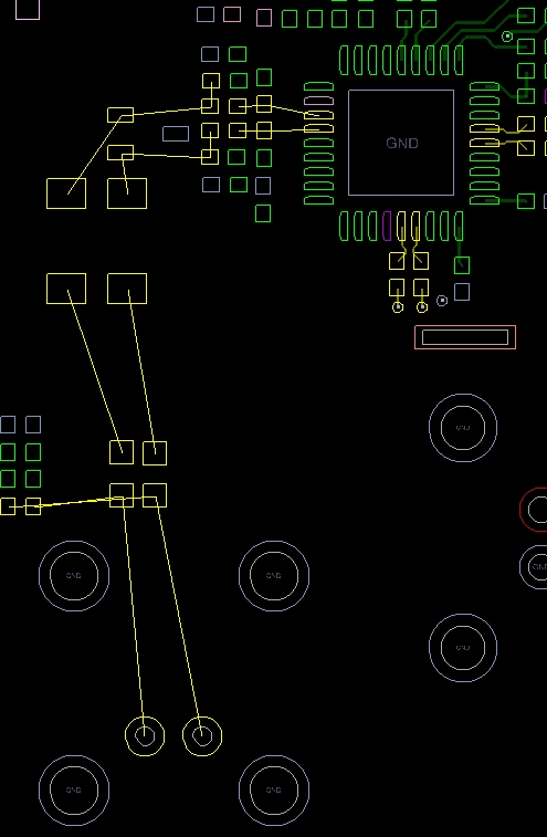
2. Does the CMC common mode inductor just need to dig out the GND on the surface?
3. How to deal with the GND of the connector? Need to dig the ground?
4. Is the length between TX and RX of SGMII required to be equal?
