This thread has been locked.

If you have a related question, please click the "Ask a related question" button in the top right corner. The newly created question will be automatically linked to this question.

DP83867IR: DP83867 MDIO control issue

Part Number: DP83867IR

My design used zynq platform with DP83867.

It is not controlled MDIO on u-boot.

I find two cases.

Case 1: get the same date for every register address.

Case 2: get the 0x0000 data for every register address.


I try to check as below:
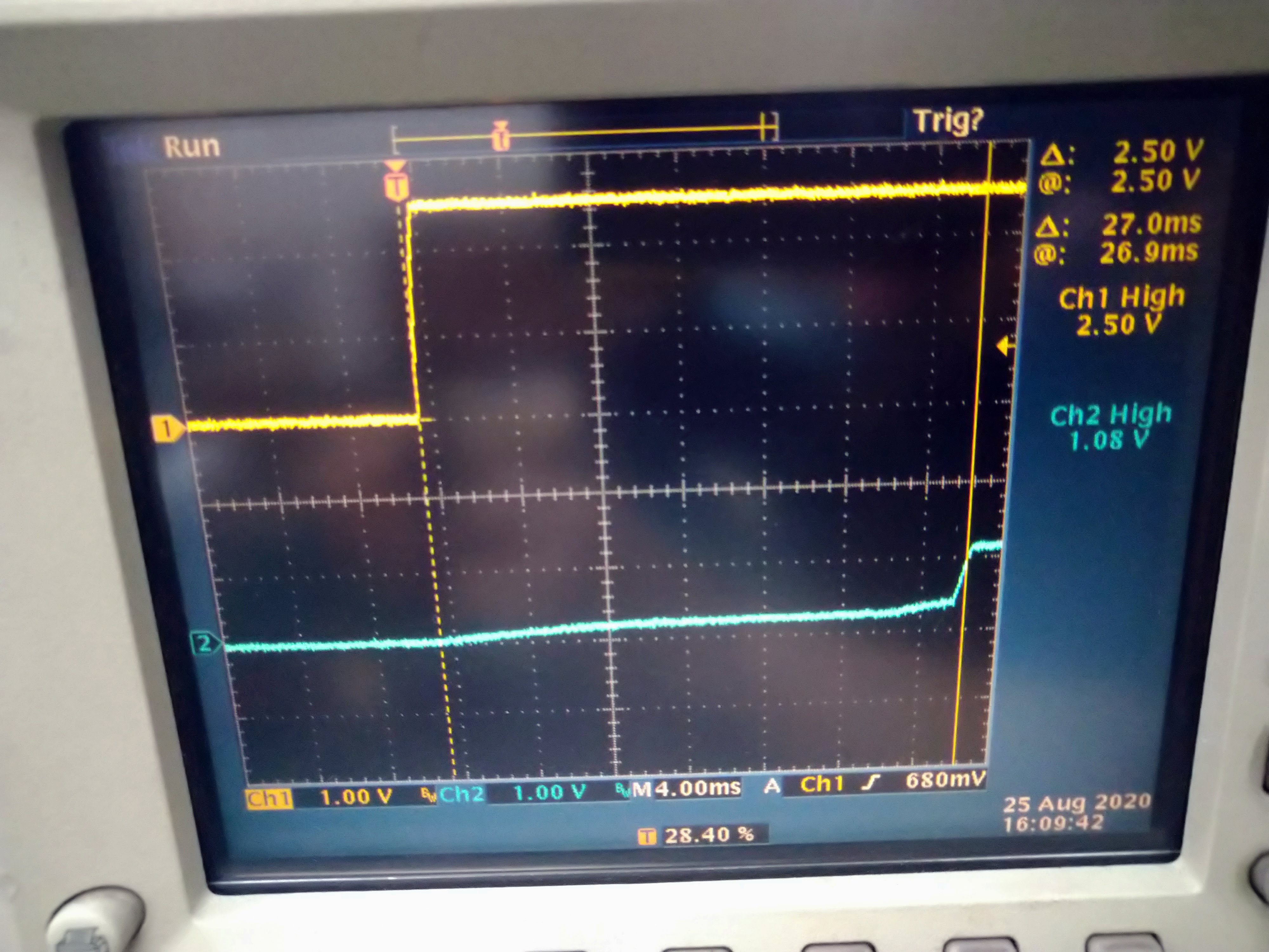
VDDIO            ==> 1.8V

VDD1P1          ==> 1.1V

VDDA2P5        ==> 2.5V

RESET             ==>1.8V

CLK_OUT         ==>25MHz

RX_CLK          ==> no signal


How to fix MDIO control issue? 
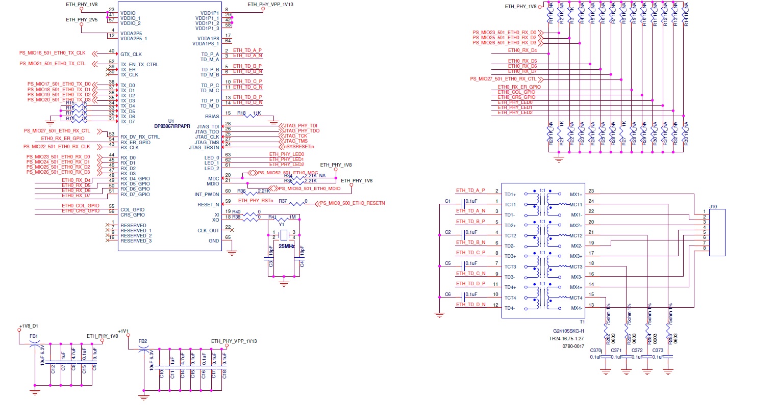
My design as below

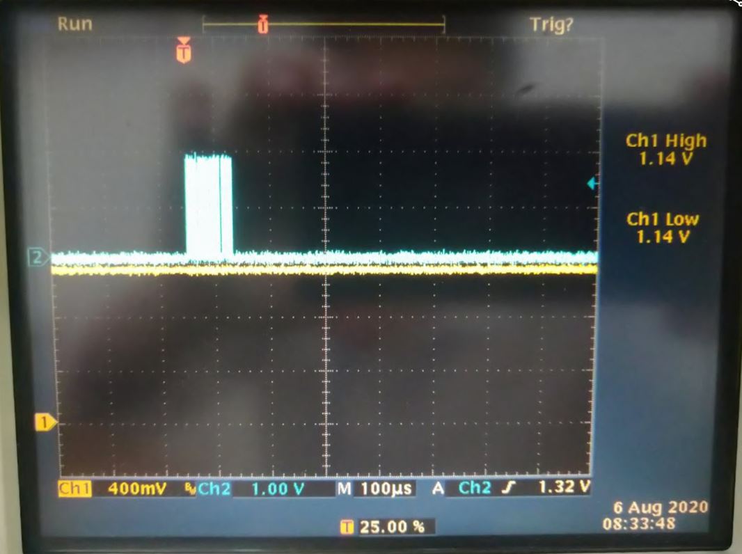
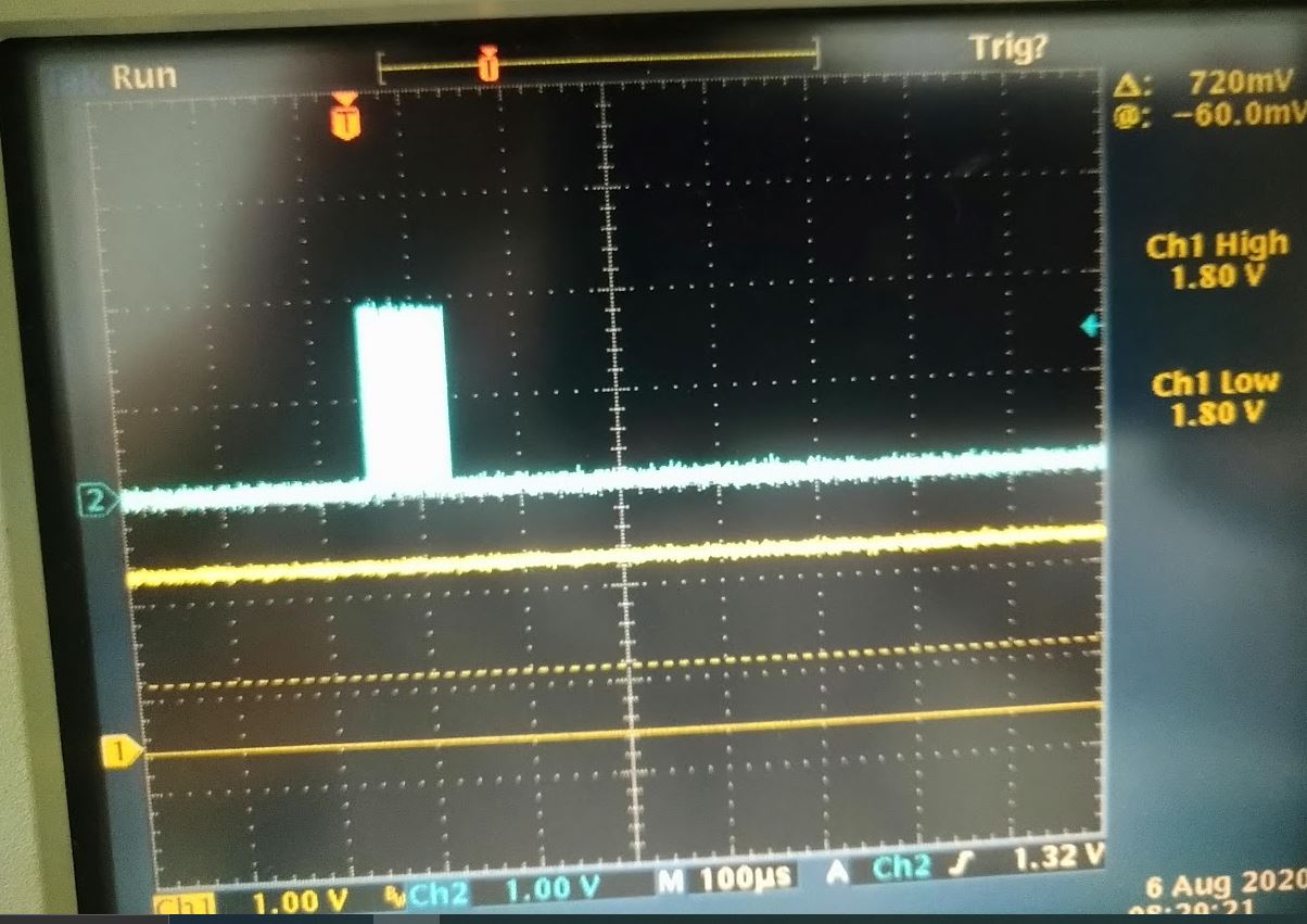
Capture MDIO waveform

  • Hello,

    Thank you for providing the schematic, the MDC, MDIO connections on the PHY look correct, 

    Can you provide the voltage the processor is running at? Can you also provide data showing multiple register reads for both case 1 and case 2 you've described?

    Regards,
    Justin 

  • Dear Justin,

    I capture waveform for you.

    Case1:

    capture register 0x1~0x5

    Zoom in package #1

    Zoom in package #2

    Zoom in package #3

    Zoom in package #4

    Zoom in package #5

    Case 2:

    Capture register address 0x0~0x05

    zoom in package #1

    zoom in package #2

    The MDIO is running and check the voltage.

    capture 1.1V and MDC

    capture 1.8V and MDC

    capture 2.5V and MDC

    Thanks

  • Hello,

    Do you have the ability to use an external TI Launchpad and the USB-to-MDIO tool to verify that you can read/write registers?

    Regards,
    Justin 

  • Dear Justin,

    I have not the USB-to-MDIO tool hardware.

    Thanks,

    SJ

  • Hi SJ,

    I'm sorry for the delayed response. I suggest using a released MDIO communication tool to verify the electrical connections on MDC and MDIO pins. The intermediate voltage shows where the PHY is expected to provide data suggest there is some contention on the MDIO output. The voltage is neither pulled high when the PHY would be inactive or to Ground when the PHY should drive low. Is the FPGA configured to accept the data the PHY provides during each read function?

    Regards,

    Justin 

  • Dear Justin,

    I have been applied to the MDIO communication tool but didn't arrivals. It needs some time.
    The u-boot function is working on another product's board for MDIO control.

    Have power on and power off sequences on this design?
    My sequences is ETH_PHY_2V5 -> ETH_PHY_1V8 -> ETH_PHY_VPP_1V13.

    Thanks,
    SJ

  • Hi SJ,

    The DP83867 does specify that VDD2P5 and VDD1P0 should ramp together and VDDIO should ramp within 50ms of the other supplies. Can you describe the time between each supply ramps up?

    Does the u-boot tool and DP83867 share a common ground?

    Regards,

    Justin 

  • Dear Justin,

    I  check the power follow as:

    2.5V(VDD2P5) -> 1.8V(VDDIO) is 23.6ms
    2.5V(VDD2P5) -> 1.1V(VDD1P0) is 26.0ms

    I check the datasheet on page 124. The datasheet has highlighted as "There is no requirement for the sequence of the supplies when operating in two-supply mode."
    What's the correct power sequence?

    The u-boot is the same elf file, but different FPGA code. This FPGA code the same configuration for the Ethernet of the part.

    Regards,
    SJ

  • Hi SJ,

    You are correct, I mistook the VDDIO = 1.8V for the VDD1P8 supply. The power sequencing looks correct. 

    Can you verify the FPGA using u-boot and the DP83867 share a common ground? The MDIO waveform should not have the intermediate voltage, this is where I would like to narrow the troubleshooting. Are you able to write to registers and verify they if they are successful, like say writing to turn on an LED?

    Regards,
    Justin 

  • Hi SJ,

    I am closing this thread since I have not heard a response. If you need assistance, please create a new post and reference this thread.

    Regards,
    Justin