This thread has been locked.

If you have a related question, please click the "Ask a related question" button in the top right corner. The newly created question will be automatically linked to this question.

SN65HVS885: SN65HVS885 question

Part Number: SN65HVS885


Hi ti team,

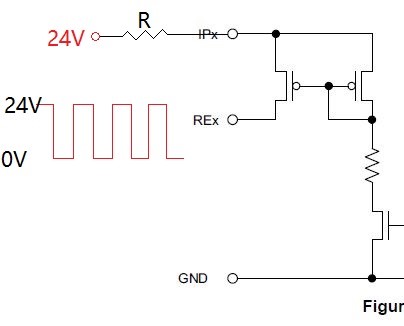
  • The recommended usage of this chip in the data sheet is shown in the figure below:

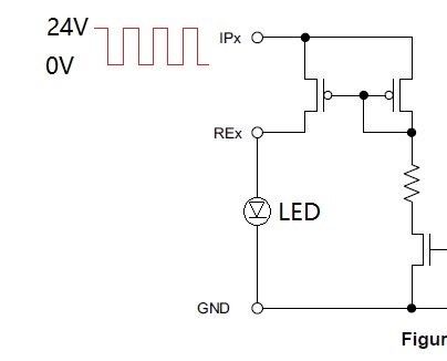
However, according to our usage scenario, we want to adjust it to the following way. Is it feasible?In addition, how much voltage can RE pin withstand?

  • Hey Jimmy,

    Am I understanding right that you're attempting to drive a 24V DC signal into the IPx inputs and are hoping to see a PWM at the REx outputs? The PWM from the input is what would be driving the LED's so this wouldn't work. If you put in the 24V DC signal on the inputs you won't see the PWM on the output. The chip itself isn't creating that signal.

    What exactly is it you're trying to perform with this function? Maybe we can find a better solution

    Rami

  • Hi  Rami,

               As shown in the figure below,If we tie the IPx to 24V DC and drive a 24V DC signal into the REx inputs ,could SN65HVS885  get this signal and send it to mcu  through it‘s interface

  • Hey Tcheng, Jimmy

    So the issue i'm seeing here is when you have the REx high.
    Here's a simplified block diagram of a single channel to help explain the issue better:


    So you see that the return current (through the limiter circuit) goes to a switch which can either select FGND or the corresponding RE output. Initially it is set to FGND, and it only switches when some conditions are TRUE. 1) the current exceeds half of the configured limit, 2) the voltage with respect to FGND exceeds the input threshold, and (3) the state is held for the duration of the debounce filter.

    When, the RE signal is at 0 V the part should detect a “high” level fine (since this is similar to the normal expected operating conditions when a field input is high and RE is grounded).  But when RE is held at 24 V it isn’t totally clear how the circuit would behave. When it transitions from 0 V to 24 V it should reduce the current below the threshold and switch the return path to from RE to FGND (resulting in a “low” state being reported).  But, when the return path is switched to GND the input would look high again (since it is above the high-level threshold and sinking enough current).  Because of this, it seems like it would keep oscillating between high and low states. 
    So overall I wouldn't expect this setup to work.

    What's the purpose of using the device this way and not the recommended way?

    Thanks,
    Rami