


Part Number: TCA9800
Other Parts Discussed in Thread: REF3430,
See attached schematic.
We are using the TCA9800 to interface an MSP430 running at 3.3V to an ADC121C02 running at 3.0 V. This 3.0V is coming from a REF3430. The 3.0V is also being used to power other circuitry.
To prolong battery life, the micro will keep the REF3430 disabled and only enable when required. The TCA9800 VCCA is 3.3V and VCCB is 3.0V. VCCA is always present but VCCB is enabled only when required as mentioned earlier.
TCA9800 enable pin is left unconnected so that it is pulled high at all times.
According to the datasheet,
"The SCLA and SDAA pins enters a high impedance stte when either VCCA or VCCB fall below their UVLO voltages".
"When VCCB falls below UVLO, the current source turns off, and a weak pull-up is connected to prevent the B 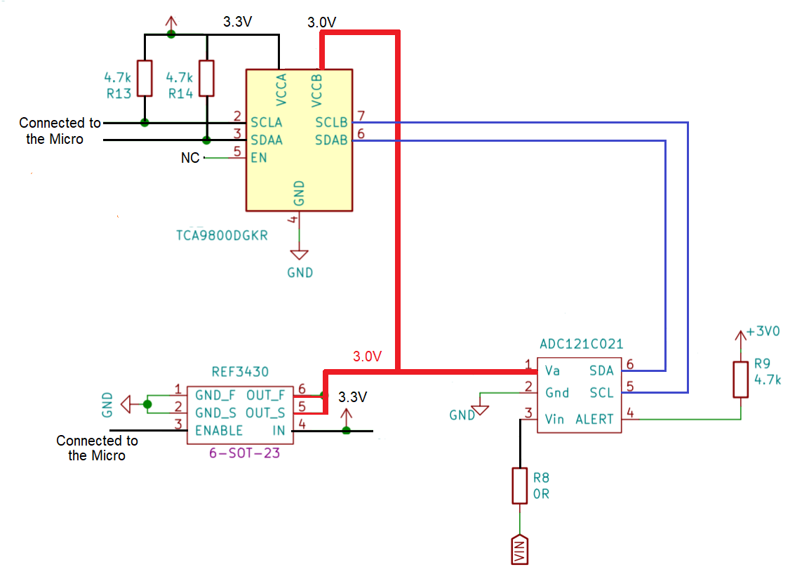 pins from floating. This is intended behavior, because no external pull-up resistors are to be used on the SDAB or SCLB pins. This behavior prevents the bus pins from floating, and allows it to follow VCCB.".
In our circuit, when the REF3430 is disabled, VCCB will be 0V which means
1) The SCLA and SDAA pins enter high impedance state preventing any leakage on the A side.
- and -
2) SDAB and SCLB will also be at 0V and since the ADC is also powered off, there should not be any scope for current leakage.
Do you see any issues with this circuit ?

