This thread has been locked.

If you have a related question, please click the "Ask a related question" button in the top right corner. The newly created question will be automatically linked to this question.

TCA9554A: How to correctly config standby mode ,all I/O need to config as input?

Part Number: TCA9554A
Other Parts Discussed in Thread: TCA9554, TCA9534A

Hi, all

There is a issue that we can't achieve our goal when we want to TCA95554A going to standby mode.

Our project need a low leakage current when in sleep mode, so we want the part of TCA9554A going to the standby mode.But when we config it as datasheet mentioned ,it didn't response a expected value. 

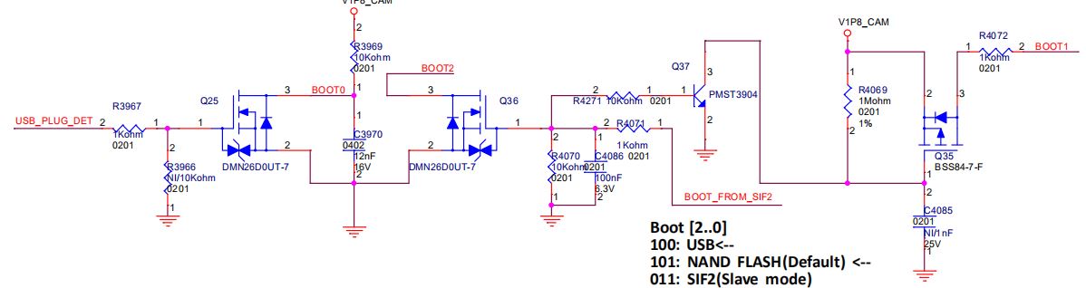
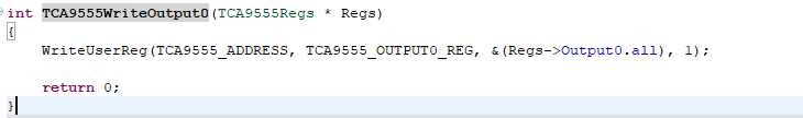
As attached is our design and code, please give me a hand .

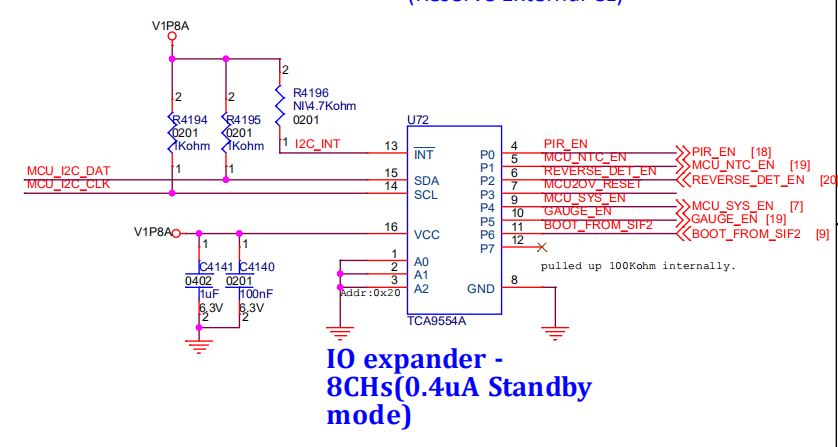
When the system is in normal mode, the TCA9554A I/O will config as outputs.

If the system  will sleep, TCA9554A I/O will config as inputs, and config the i2c freq to 0 kHz.

And I have tried different conditions, step by step ,1 ===> 2 ===> 3 ===> 4 ===> 5

POWER SUPPLY : 4 V

Operation TCA9554 Current (NORMAL) TCA9554A  Current (SLEEP) POWER SUPPLY Current  (NORMAL)  (A) POWER SUPPLY Current (SLEEP) (A)
1. NO HW Change 0.023889A 0.000199A 0.136 0.109
2. P0-P7 pull-up to 1.8v with 1k R 10.08uA 15.33uA 0.032 0.023
3. Disconnect P0-P7 R(expect P4(SYS_EN) -0.99uA 4.75uA
4. Disconnect pull-up 1.8v 16.8uA 17.44uA
5. Disconnect pull-down R in P4(SYS_EN) 1.04uA -4.2uA 0.129 0.110

 Another DUT do 2345 -1.06uA 5.6uA 0.124 0.113

So could you tell me how to achieve the datasheet mentioned type value?

I have tested config all I/O as inputs, I2C freq to 0 kHz , and pull up the input, whether is it a SW issue or HW issue?

And during the test, disconnecting the TCA9554A VCC, Voltage measured from VCC still is 1.8V , can you tell me why?

Sincerely,

Jay

  • Hi Jay,

    The most common cause of higher-than-expected ICC on this device is having an input port that is left floating or otherwise biased to some intermediate voltage rather than VCC or GND.  I saw that you mentioned tying the inputs high and it not resolving the issue, but from your table it looks like they may have been pulled up to 1.8 V while VCC is at 4 V.  Could you please try pulling the inputs to VCC?

    Regards,
    Max

  • Hi, Max

        Thanks for your reply.

        I think there maybe some misunderstand that 4 V is a system voltage,not the TCA9554A VCC.  The VCC of TCA9554A is V1P8A as last attached. Am I right?

         Or I should test TCA9554A Vcc = 1.8V, pull up inputs to 4 V?

         And there are some confusing condition : Should I pull up all I/O to TCA9554A Vcc for into standby mode?   Like : P0 ,P1.P2,P3,P4,P5,P6,P7 = 1.8 V  or  I/O just need to config to a certain level , Vcc or GND, like P0,P1,P3,P5 = 1.8 V P2,P44,P6,P7 = GND ?

    Sincerely,

    Jay

  • Hi Jay,

    Sorry for my misunderstanding about the VCC rail.  If it is 1.8 V then you do not need to pull the input ports to any higher voltage.

    The datasheet defines ICC for different states of the Px ports.  When they are all pulled to VCC, the typical ICC is 0.4 uA.  When they are all pulled to GND, the typical ICC is 230 uA.  (It is higher here because of the integrated 100-kOhm pull-up resistance.)  This assumes a 1.95-V supply (i.e., 1.8 V plus some tolerance).  If the voltage is between VCC and GND, the current could be higher.  This is because the input circuitry is like a CMOS inverter which could have some shoot-through current at mid-level inputs (see this app note for further details: https://www.ti.com/lit/an/scba004d/scba004d.pdf).

    When you disconnect all the circuitry it looks like the current is lowest, which makes sense given that based on your application this seems to be the only case where all inputs would be assured to be at a high level.  The thing that seems a little strange is that the measured value is close 1 uA, which is the expected maximum value for TCA9554A.  (Normally under nominal conditions like room temperature testing I would expect results closer to the "typical" values than the "maximum" ones.)  Just to confirm - is your current measurement able to measure only the TCA9554A contribution, and is it accurate to within a fraction of a uA?  (I ask about the accuracy since I see in some cases a negative current - I'm not sure how to interpret that.)

    Regards,
    Max

  • Max,

    I also have customer mentioned this concern, they need lower standby current compared to TCA9554A, so can you suggest suitable one to me?

    Is there open-drain topology I/O expander?

    Thanks

  • Paul,

    Actually, any IO expander could be used as an open-drain output.  You would just configure a port as a low output to drive a "low" state or configure it as an input whenever it needs to be high-Z (so that it could be pulled high externally by a pull-up resistance).  If the customer is seeing higher standby current due to the internal pull-up resistances (i.e., if inputs are held low), though, then they might want to try an expander without these integrated.  Also, make sure that input ports are biased fully high or low as discussed previously in this thread to achieve the lowest possible ICC.

    Max

  • Max,

    Thanks for explanation.

    But if customer don’t prefer external pull high resistor and need standby current lower than TCA9554A, do you have any suggestion? Or this device is the best  choice?

    Thanks

  • Hi,Max

         Thanks for your explain in detail.

          And now,we just want to use a IO expander as GPIO output like the Schematic Diagram drawed,it looks like TCA9554A not Conforming to the requirements.

         So could you recommend another IO expander  which can be used for  our design and achieve standby mode even though I/O will pull down?

    Best regards,

    Jay

  • Hi,Max

        I have found the TCA9534A from TCA9554A datasheet, what's your comments for it? It looks like good that is same as TCA9554A expect pull up R.

    Thanks,

    Jay

  • Jay,

    You are correct - these devices are the same except for the presence of internal pull-ups on TCA9554A which are not in TCA9534A.

    Max