This thread has been locked.

If you have a related question, please click the "Ask a related question" button in the top right corner. The newly created question will be automatically linked to this question.

DP83822I: DP83822I eye test failure(Twisted Pair Active Output Interface template)

Part Number: DP83822I

Hi, Team

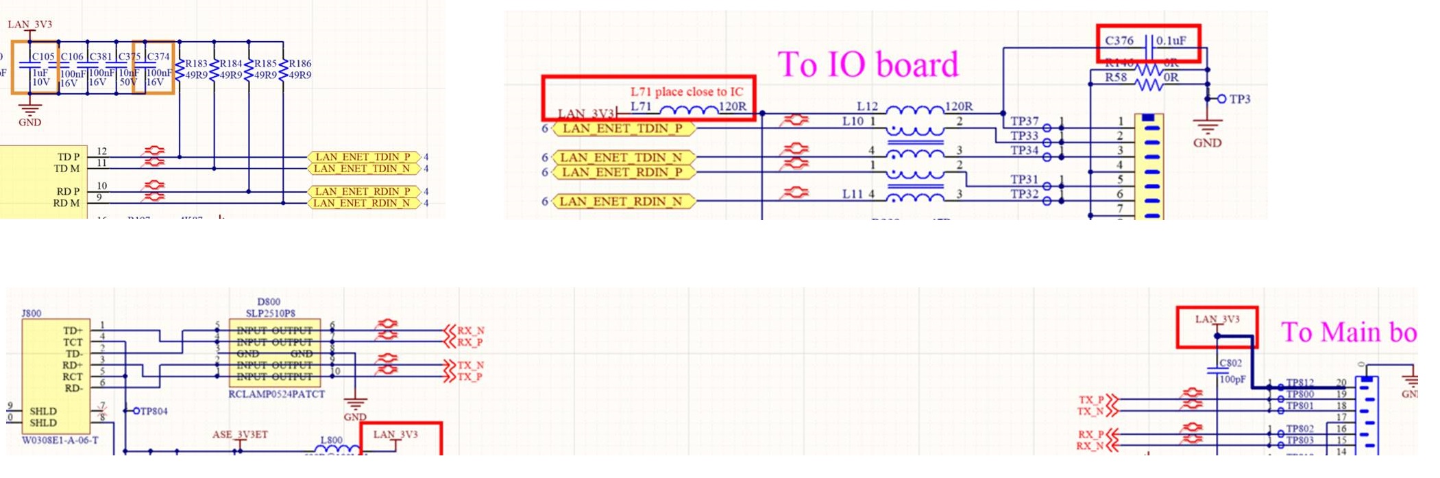
Our customer using DP83822I in the smart speaker, and they we meet the eye test failure( Twisted Pair Active Output Interface template).

Test report pls check the attach file.

Also, they using our DP83822I EVM connect to their MCU board, the eye test ( Twisted Pair Active Output Interface template) pass.

I am not sure whether it’s relate to any filter in the SCH.

Could u help to check and give some suggestions?

Thanks.


G.W

tokyo enet-fail.pdf

  • Hi GW, 

    The mask failures you've described could be the result of the physical layout or component selection in the application. I've included some items that could be contributing below: 

    1. Can you describe the tolerance on the MDI 49.9ohm pull-up resistor and RBIAS? We would like these to be 1% tolerance.
    2. What is the trace length between the DP83822 and RJ45? This should be kept as short as possible.
    3. We don't recommend using on the pull-up of the center-tap pins of the RJ45/Magnetic. Can you try shorting this component and viewing the results?
    4. Are there other sources of additional capacitance on the MDI lines of the board?

    Regards,
    Justin 

  • Hi, Justin

    Thanks your suggestions, pls check customer feedback as below. Pls help to check and give some suggestions, thanks.

    Question 1:Can you describe the tolerance on the MDI 49.9ohm pull-up resistor and RBIAS? We would like these to be 1% tolerance.

    GW: Customer confirm the MDI pull up resistor is 1% tolerance.

    Question2: What is the trace length between the DP83822 and RJ45? This should be kept as short as possible.->

    GW:There are two connectors and FPC cable between the DP83822 and RJ45 , the trace length between the DP83822 and connector J4A is 151mm,the length of FPC cable is 150mm, the trace length betweenJ4B is 30mm.So the length between the DP83822 and RJ45 is about 331mm


    Question3: Are there other sources of additional capacitance on the MDI lines of the board?

    GW: do you mean RD+-/TD+- to RJ45?

    RD/TD->common chock-> connector J4A-> FPC cable-> connector J4B->TVS D800-> RJ45.

    for cable length, pls ref Question 2.

    Best Regards

    GW

  • Hi GW,

    I would like to clarify my 3rd question above. TI does not recommend using an inductor between the center-tap pull-up resistors and VDDA supply.

    Is the FPC cable you are using impedance controlled to 100ohms differential? The length between the PHY and the compliance test point is very long. The purpose of the compliance testing is to test the output of the PHY, with minimal impedance imbalance points as possible. This way the transmitter of the PHY can be verified to be in compliance, like what you are seeing with the EVM. 

    Moving forward, you can try shorting the inductor but the long trace length, connectors, and cabling between the PHY and the RJ45 makes it difficult to measure the output of the PHY without introducing additional variables.

    Regards,
    Justin 

  • Hi, Justin

    Thanks your suggestions.

    And I just prefer to double confirm with the inductor, do u mean to shorting L815 as below?

    Thanks.

    G.W


  • Hi GW, 

    I am referring to L800 and replacing it with a 0ohm resistor.

    Regards,
    Justin