


Part Number: TS3USB30E
Hi,
I'm designing a "USB Switch" based on TS3USB30E IC, I not have experience on Diff pairs signal routing. I tried to base my design on guidelines of the app note SPRAAR7H but I have some questions.
Application:
USB switch, of one side connects the PC and a usb device to the other.
PCB:
2 Layers FR-4
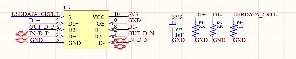
Schematic:
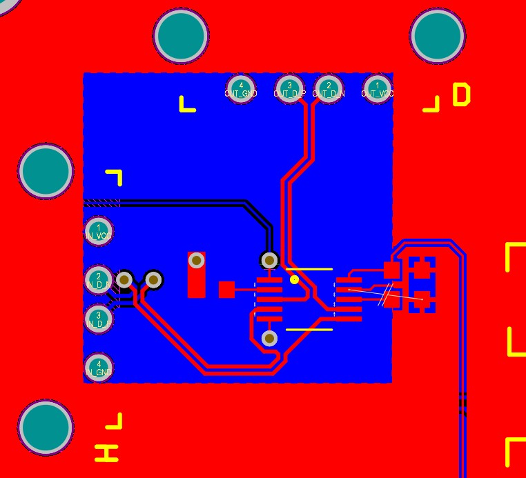
Layout:
I will change the Female USB A type for the input to a micro USB :)
Questions:
1.- I'm little confused about the ground planes, so it's ok to cut out the gnd plane on the top where the USB signal be and let the bottom gnd plane as the reference plane?
2.- I set the impedance ctrl in altium to 90 ohms / 15% tolerance,so theoretically the traces are on this range, is that ok?
3.- I set the min length to 4000 mils and the max length to 12000 mils but I'm far away from this length, because my space is limited, on the app note not mentions a minimal length, what's involved that the lengths be under 4000 miles?
Thanks for the support!
